DEEP RESEARCH · NAVITAS SEMICONDUCTOR (NVTS) / 800VDC GaN & SiC
Navitas Semiconductor: The 800VDC AI-Power Transformation and the 'Navitas 2.0' Inflection Point
4Q25 is the revenue bottom, high-power crosses 50% for the first time — the purest beneficiary of the Rubin/Kyber 1MW rack cycle
0. Bottom line first
Navitas Semiconductor's (NVTS) 4Q25 is not weakness — it is a structural inflection. Mobile revenue was deliberately cut by more than half, but the high-power segment crossed 50% of quarterly revenue for the first time, with Non-GAAP gross margin holding firm at 38.7%. About $450M of design-win backlog and $236.9M of cash with zero debt are the safety net that carries the company to the Nvidia Kyber/800VDC mega-cycle. The trailing P/S of 35–49x is an optical illusion — a contrarian entry point. Recommendation: Buy & Hold.
1. Investment summary and the market's mispricing
The most powerful macro theme in IT hardware and semiconductors is "breaking the power-density wall" in AI data centers. LLMs and Agentic AI turn data centers into "AI factories," and Nvidia GPU rack power explodes from kilowatts to megawatts. Transition to 800VDC (high-voltage DC) architecture is no longer a choice but a survival requirement — and Navitas, a GaN/SiC leader, sits at its center.
The market severely mispriced the intrinsic value. As of 4Q25, the stock was anchored on trailing Chinese mobile/low-end charger revenue collapse, with short interest reaching ~21%. But 4Q25 is not merely a trough; it is the structural inflection point where fundamentals fundamentally reverse.
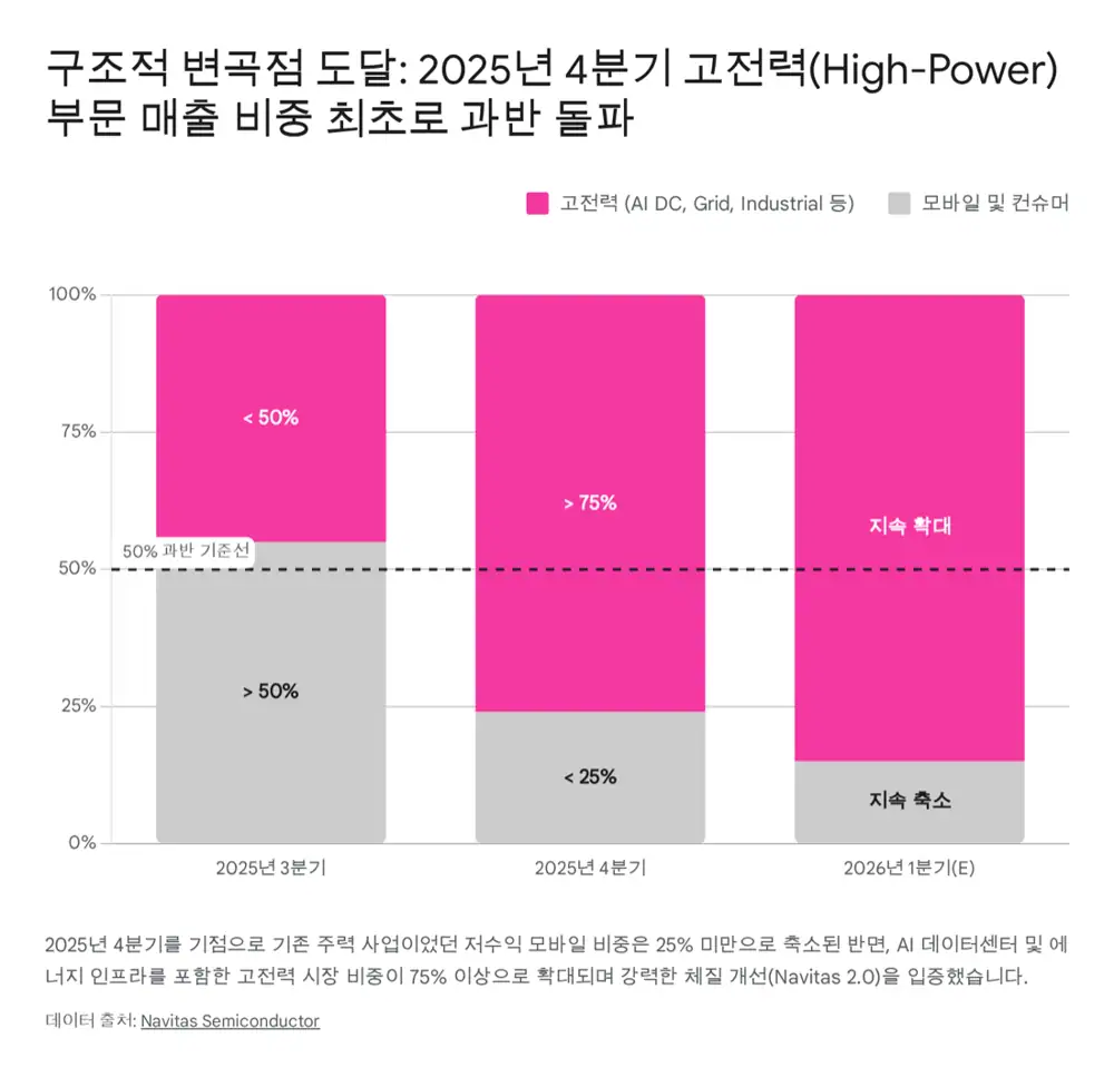
The 'Navitas 2.0' strategy explicitly trims mobile and reallocates to four high-power markets: ① AI data centers, ② energy/grid infrastructure, ③ high-performance computing (PC), ④ industrial electrification. As a result, in 4Q25 high-power crossed the majority of quarterly revenue for the first time, with a cumulative design-win backlog around $450M.
2. Intrinsic moat: GaNFast monolithic + 5th-gen GeneSiC
2.1. Technical edge over physical limits
Legacy silicon (Si) MOSFETs that dominated the power industry for half a century generate excessive switching loss and heat in >1,000W GPU racks, putting fatal pressure on data-center thermal management. Gallium nitride (GaN), by contrast, has a 3.39 eV bandgap (vs. Si's 1.12 eV) and overwhelmingly higher electron mobility, ideal for ultra-fast switching and high-density conversion.
Discrete GaN parts have fragile gates, risking ringing and shoot-through at high frequencies. Navitas industry-first commercialized monolithic integration of pure GaN power devices with gate drive, control and protection circuits on a single silicon die — the GaNFast™ and GaNSafe™ power ICs.
- Autonomous protection detecting/blocking faults within 50 ns + up to 2kV ESD protection, with no extra board space.
- Switching frequency lifted to 1MHz allows replacing bulky wound LLC transformers with planar transformers. Within the CRPS/OCP form factor, PSU power density jumps from 98 W/in³ to 137 W/in³.
On SiC, the 5th-gen GeneSiC™ platform with patented Trench-Assisted Planar (TAP) architecture combines planar stability with trench density. From 1.2kV to 3.3kV, it delivers industry-leading thermal characteristics and top-side cooling packaging, making Navitas content effectively mandatory in AC-DC conversion, SSTs and megawatt BESS.
2.2. Fabless model and supply-chain restructuring
Unlike IDMs (Infineon, ST, onsemi), Navitas is pure fabless. In a compound-semiconductor transition, this delivers technical agility without massive CAPEX burden. The recent foundry reshuffle turned scale/cost from weakness into strength.
- Diversification ahead of TSMC's July 2027 exit: Partnership with Taiwan's PSMC (Powerchip) to develop 200mm (8") GaN-on-Silicon on an enhanced 180nm CMOS process. Going from 150mm → 200mm cuts per-chip cost and improves yield. Migration begins with 100V products in 1H26 and extends to the 650V family.
- Geopolitical diversification: Long-term partnership with GlobalFoundries (GF). Mass production in GF's Vermont fab begins in 2H26. Locks in 'Made in USA' premium for US data centers and defense systems.
3. End-market deep dive: physical necessity of 800VDC
3.1. The fall of 54V and the move to 800VDC
The decisive driver for explosive 2026–2030 growth is the data-center power-grid paradigm shift triggered by Nvidia Blackwell and Rubin.
- GB200 NVL72: 72 Blackwell GPUs + 36 Grace CPUs, 120–132 kW per rack.
- GB300 NVL72: about 150 kW per rack.
- From 2027, Rubin Ultra-based Kyber racks: 1,000 kW (1 MW)+ per single rack.
By P=VI, delivering 1MW at 54V requires 18,500 A, sending I²R losses through the roof. 1MW per rack needs ~200kg of copper busbar; a 1GW AI data center would need 500,000 tons of copper just for rack-internal busbars — sourcing and floorspace become impossible. PSUs eat up to 64U of rack space, leaving no room for compute trays.
The standard that breaks this, proposed with OCP, is the 800VDC HVDC architecture: convert 13.8kV grid power once to 800VDC at the data-center entrance (SST/industrial rectifiers) and feed it directly to racks. Stepping voltage 15× from 54V to 800V cuts current to 1/15, and copper weight crashes from 200kg to ~18kg (40 lbs) — a 95%+ reduction. Eliminating conversion stages improves end-to-end efficiency by up to 5% and reduces maintenance cost by up to 70%.
| Metric | Legacy 54VDC | 800VDC (Kyber) | Implication |
|---|---|---|---|
| Conversion path | Grid → multi AC/DC → 54V → multi DC/DC → GPU | 13.8kVAC → central 800VDC → direct → single DC/DC → GPU | End-to-end efficiency up to +5% |
| Current at 1MW | ~18,500 A | ~1,250 A (1/15) | I²R loss and heat collapse |
| Copper per rack | ~200 kg | ~18 kg | Lower copper cost & less space |
| Rack space | Power shelves consume up to 64U | PSU consolidation/miniaturization | Power density 137 W/in³+ |
| Operations & maintenance | Multiple PSUs and fans → high failure rate | Simpler structure → -70% maintenance | TCO optimization |
| Core devices | Silicon (Si) | GaN / SiC | WBG specialists like Navitas required |
3.2. Navitas's core positioning
All-GaN DC-DC brick
800V → 50V/12V step-down IBC. The 10kW 800V-to-50V All-GaN platform integrates 650V and 100V GaNFast FETs in a 3-level half-bridge with synchronous rectification. 1MHz switching shrinks magnetics; in a 61×116×11mm full-brick package it delivers 2.1 kW/in³, the industry's highest power density. Peak efficiency 98.5%, full-load 98.1%.
HV SiC SST
SSTs and MW rectifiers bridging 13.8kV+ grid to 800VDC. 5th-gen GeneSiC 1.2/2.3/3.3kV SiCPAK™ module portfolio. Intensive sampling/evaluation with 15+ global OEMs.
NVIDIA 13-vendor consortium
Officially included in the exclusive 800VDC vendor consortium alongside Infineon, ST, onsemi and TI. The only WBG pure-play covering both high-voltage GaN and HV SiC.
3.3. Five-year TAM outlook
Management and market researchers expect the SAM across the four high-power targets to grow at a 2025–2030 CAGR of 60–75%, reaching $3.5–$5.4B in 2030. GaN and HV SiC split roughly 50/50. The AI data-center power-semi sub-segment alone reaches $2.5–$2.6B per year by 2030. As Kyber racks roll out at scale from 2027, early component orders should start to flow in 2H26, with explosive revenue recognition starting 2H26.
3.4. Risks
- Innoscience competition + patent disputes: China-based Innoscience built early 8" GaN capacity and leads global volume share. The ITC's recent initial ruling in Infineon vs. Innoscience favored Innoscience, removing legal uncertainty and intensifying mobile/general-adapter price competition. But Navitas's focus — 800VDC primary-side and 3.3kV SiC — is governed by extreme reliability/lifetime requirements, limiting low-end pricing pressure.
- Hyperscaler in-house silicon + qualification delays: AWS Trainium, Google TPU, Microsoft Maia and similar in-house accelerators could splinter TAM if their architectures don't 100% adopt 800VDC. Some research notes that Navitas's newest products may take time to fully clear Tier-1 mass-production qualification.
4. 4Q25 results: bottom confirmation and qualitative pivot
4.1. The numbers and the big-bath nature
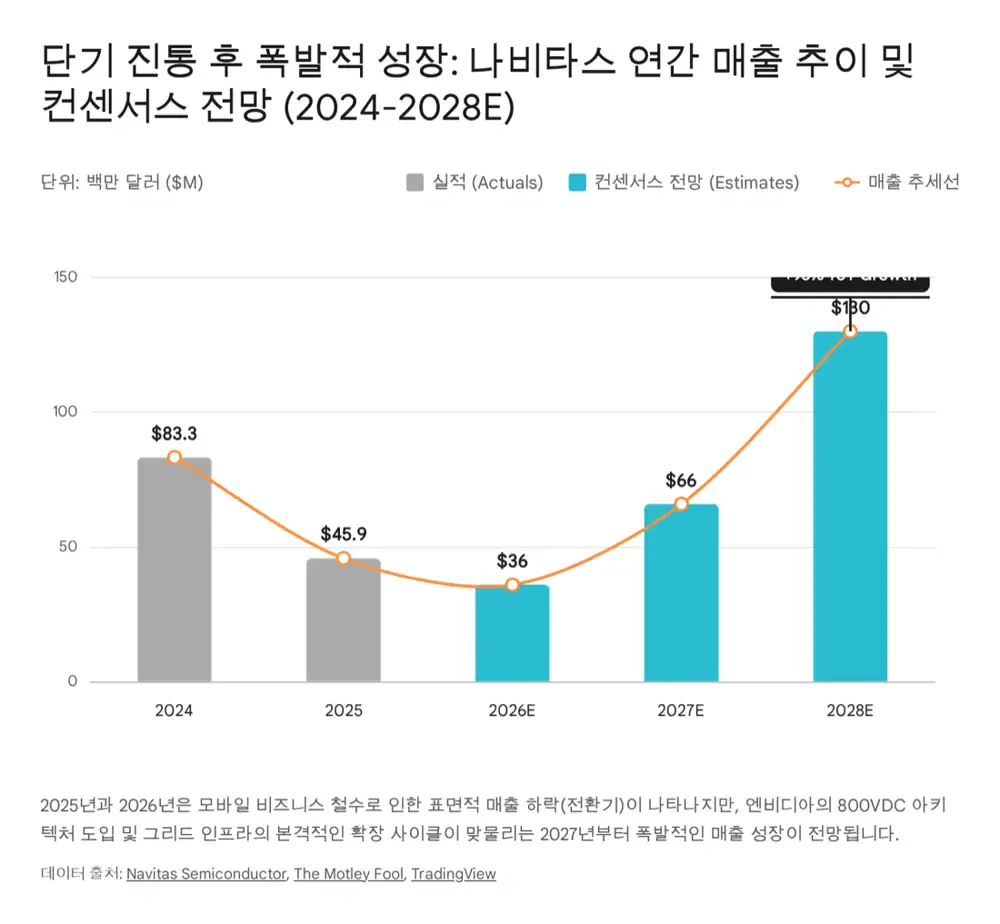
- Revenue: 4Q25 $7.3M (vs. 3Q25 $10.1M; YoY -59%). FY2025 $45.9M (vs. $83.3M; -45%).
- GAAP operating loss: 4Q25 -$41.4M — including a 'Big Bath' one-off. Restructuring & impairment of $16.6M (mobile-exit distributor termination ~$10M + impaired surplus fixed assets ~$4M + severance for 19% headcount cut ~$2M; only $3.8M non-cash).
- Non-GAAP operating loss: ~$12.1M — no fundamental breakdown.
4.2. Dramatic revenue mix reversal = Navitas 2.0 validated
Low-margin, fiercely competitive mobile, which was >50% of revenue through 3Q25, collapsed to under 25% of total revenue in 4Q. Conversely, high-power — covering AI data-center power solutions, SSTs and megawatt adapters — became the majority of quarterly revenue for the first time in company history. The distributor network was consolidated from ~40 Asia-focused generic vendors down to fewer than 10, with strategic partners like WT Microelectronics and Avnet (enterprise/industrial specialists).
CEO Chris Allexandre: "Q4 is the true bottom, and low-margin mobile will fade to immaterial by end of 2026." 1Q26 guidance: $8.0–$8.5M — the first QoQ growth turnaround since the pivot announcement.
4.3. Profit visibility and operating efficiency
Despite the worst possible scale absorption, Non-GAAP gross margin held firm at 38.7%. The 19% headcount cut streamlined SG&A while redeployment funded core US-based high-power engineering/sales talent. Management guided to roughly $15M/quarter of OpEx through 2026 — a tightly controlled cost base that means gross profit will burst through fixed costs once revenue inflects, completing a textbook operating-leverage setup.
5. Q, P, C dynamics
| Earnings dynamic | Key drivers | Financial impact |
|---|---|---|
| Q (shipments & content) | Full Rubin (Kyber) 1MW rack adoption; rack/MW dollar content explodes ($25k–$35k) | Gradual monetization of $450M backlog; explosive top-line from 2027 |
| P (premium pricing) | 98.5% peak-efficiency 10kW module; system-level TCO cut (less heat, -70% maintenance) | Hold high-margin premium policy vs. commodity parts; lifts gross margin |
| C (cost & leverage) | PSMC 200mm wafer migration (1H26); post-restructuring fixed OpEx of $15M/quarter | Per-chip cost reduction; dramatic EBITDA break-even on revenue rebound |
Q: A 12V general server rack carried only a few hundred dollars of power-semi content; a Blackwell GB200 NVL72 rack is a $3M super-rack with GaN and SiC injected at every conversion stage. Management estimates next-gen infrastructure TAM at $25,000–$35,000 of content per MW, plus another $10,000–$12,000 of SiC per MW on the external SST/BESS side. Hyperscalers building dozens of gigawatt AI factories drive 'Q' on a power-law curve from 2H26.
P: In mission-critical applications, efficiency and reliability drive premium pricing. For MW-scale operators, every 0.1% efficiency gain saves millions in electricity and avoids huge cooling-system expansions. 98.5% peak efficiency and 1MHz switching make chip-level $-difference irrelevant — a system-level TCO moat.
C: 200mm wafers carry 77%+ more area, raising good-die yield non-linearly and maximizing fixed-cost dilution. With OpEx capped at ~$15M/qtr and revenue crossing $30–40M/qtr, ~40% gross margin punches through fixed costs and EBITDA inflects sharply.
6. Balance sheet, valuation, conclusion
6.1. Solid financial runway
As of Dec 31, 2025, cash and equivalents reached $236.9M, including a successful November 2025 private placement that added $95.6M. The company holds zero debt. Given a quarterly cash burn of $10–15M, no external financing or dilutive issuance is needed to reach the 800VDC mega-cycle in 2027.
6.2. Valuation — short-term optical illusion meets forward multiple compression
Trailing 12-month P/S is roughly 35–49x. Compared with Infineon, ST and onsemi at 5–11x, this looks like extreme overvaluation on the surface, fueling ~21% short interest. But the high P/S is the result of intentionally cutting mobile revenue (2024 $83.3M → 2025 $45.9M, roughly half) — the denominator artificially shrank.
- Street consensus revenue: 2027 $66M (+80% YoY), 2028 $130M (+96%).
- As the $450M design-win backlog converts to revenue, forward EV/Sales for 2027–2028 compresses toward normal industry levels.
- Pure-play WBG premium: Unlike legacy-burdened IDMs, Navitas absorbs the full growth beta of the AI data-center super-cycle and grid rebuild.
- Wolfspeed contrast: Owned SiC tech but was crushed under debt and CAPEX, ending in restructuring and Chapter 11. Navitas — fabless, debt-free, entering top-line expansion — is structurally different.
6.3. Near-term catalysts
- APEC 2026 (late March 2026, Texas): Official debut of the 10kW all-GaN DC-DC platform; technology validated.
- 1Q26 results: QoQ turnaround guidance ($8.0–8.5M) needs to convert into numbers.
- 200mm production + GF US production: Sequential announcements on PSMC line ramp and GF Made-in-USA test completion strengthen profitability and reduce geopolitical risk.
6.4. Conclusion
Navitas Semiconductor (NVTS) has transformed from an "ordinary consumer-grade GaN charger-chip vendor" into a "core infrastructure partner that breathes life into global hyper-AI factories and re-engineers national grids" — Navitas 2.0. 4Q25 isn't just a revenue down quarter; it is the structural bottom and the true starting point of the long-term growth story, with revenue mix completely reversed toward high-margin, high-growth high-power.
The 800VDC transition forced by Nvidia GB200/GB300 NVL72 and the upcoming megawatt-class Kyber racks isn't optional — it is the inevitable result of Joule's Law making silicon obsolete and mandating GaN and SiC. With $200M+ liquidity, zero debt, and a 1MHz/98.5% efficiency tech moat, Navitas is ready to capture the MW data-center market and the multi-trillion-won TAM that opens in 2027–2028. Treat the optical illusion of mobile revenue decline and inflated trailing multiples as a contrarian entry point and accumulate Navitas as the purest beneficiary of the AI and grid super-cycle: Buy & Hold.
Sources
- Original Naver Blog post: https://m.blog.naver.com/PostView.naver?blogId=star_of_self&logNo=224199377106
- NVIDIA 800 VDC Architecture: https://developer.nvidia.com/blog/nvidia-800-v-hvdc-architecture-will-power-the-next-generation-of-ai-factories/
- Rising power density - Goldman Sachs: https://www.goldmansachs.com/insights/articles/rising-power-density-disrupts-ai-infrastructure
- Building the 800 VDC Ecosystem - NVIDIA: https://developer.nvidia.com/blog/building-the-800-vdc-ecosystem-for-efficient-scalable-ai-factories/
- Redefining Data Center Power - Navitas whitepaper: https://navitassemi.com/wp-content/uploads/2025/10/Redefining-Data-Center-Power-GaN-and-SiC-Technologies-for-Next-Gen-800-VDC-Infrastructure.pdf
- Navitas 800VDC - Semiconductor Today: https://www.semiconductor-today.com/news_items/2025/oct/navitas-151025.shtml
- NVTS short interest - Finviz: https://finviz.com/quote.ashx?t=NVTS&ty=si
- Should You Buy Navitas - Motley Fool: https://www.fool.com/investing/2025/12/06/should-you-buy-navitas-stock-before-2026/
- Navitas 2024 results - SEC: https://www.sec.gov/Archives/edgar/data/1821769/000182176925000005/exhibit991-navitassemicond.htm
- Infineon whitepaper - Scaling AI Data Center Power: https://www.infineon.com/assets/row/public/documents/24/59/whitepaper-scaling-ai-data-center-power-delivery-with-si-sic-and-gan.pdf
- Navitas data center page: https://navitassemi.com/datacenter/
- Navitas at APEC 2026 - GlobeNewswire: https://www.globenewswire.com/news-release/2026/02/26/3245578/0/en/Navitas-to-Exhibit-Breakthrough-Solutions-for-AI-Data-Center-Grid-and-Energy-Infrastructure-Performance-Computing-and-Industrial-Electrification-at-APEC-2026.html
- Navitas 10-K - Stock Titan: https://www.stocktitan.net/sec-filings/NVTS/10-k-navitas-semiconductor-corp-files-annual-report-4a9e4aab1de4.html
- GF + Navitas - TrendForce: https://www.trendforce.com/news/2025/11/27/news-globalfoundries-moves-on-gan-tsmc-and-navitas-ties-position-u-s-as-new-gan-production-hub/
- Navitas + PSMC 200mm GaN - Semiconductor Today: https://www.semiconductor-today.com/news_items/2025/jul/navitas-psmc-020725.shtml
- Navitas 200mm with PSMC: https://navitassemi.com/navitas-announces-plans-for-200mm-gan-production-with-psmc/
- Navitas + Powerchip - Investing.com: https://www.investing.com/news/company-news/navitas-partners-with-powerchip-for-200mm-gan-production-93CH-4120112
- Navitas Q4 & FY2025 - Stock Titan: https://www.stocktitan.net/news/NVTS/navitas-semiconductor-announces-fourth-quarter-and-full-year-2025-9ije2n0e0o11.html
- GF-Navitas US GaN - REW: https://www.renewableenergyworld.com/power-grid/globalfoundries-and-navitas-gan-next-gen-power-applications/
- GF-Navitas press release: https://gf.com/gf-press-release/globalfoundries-and-navitas-semiconductor-partner-to-accelerate-u-s-gan-technology-and-manufacturing-for-ai-datacenters-and-critical-power-applications/
- GF + Navitas - Semiconductor Today: https://www.semiconductor-today.com/news_items/2025/nov/gf-navitas-201125.shtml
- Data Center infra market - IoT Analytics: https://iot-analytics.com/data-center-infrastructure-market/
- HPE GB200 NVL72 QuickSpecs: https://www.hpe.com/psnow/doc/a50009224enw
- GB200 NVL72 - Uvation: https://marketplace.uvation.com/nvidia-gb200-nvl72-ai-servers/
- GB300 NVL72 power - Sunbird: https://www.sunbirddcim.com/blog/how-much-power-does-nvidia-gb300-nvl72-need
- Scaling AI Sustainably - Murata: https://article.murata.com/en-us/article/scaling-ai-sustainably
- Gigawatt AI factories - NVIDIA: https://blogs.nvidia.com/blog/gigawatt-ai-factories-ocp-vera-rubin/
- Nvidia MW racks - Tom's Hardware: https://www.tomshardware.com/tech-industry/nvidia-to-boost-ai-server-racks-to-megawatt-scale-increasing-power-delivery-by-five-times-or-more
- Navitas Supports 800 VDC for NVIDIA: https://navitassemi.com/navitas-supports-800-vdc-power-architecture-for-nvidias-next-generation-ai-factory-computing-platforms/
- Nvidia consortium 800V - eeNews Europe: https://www.eenewseurope.com/en/nvidia-consortium-pushes-800v-power-distribution-for-ai-datacentres/
- SiC MOSFETs + AI DC efficiency - EEPower: https://eepower.com/industry-articles/how-sic-mosfets-address-ai-data-center-efficiency/
- 800-VDC shift - EDN: https://www.edn.com/the-shift-to-800-vdc-power-architectures-in-ai-factories/
- Flex + NVIDIA 800 VDC: https://flex.com/resources/advancing-the-transition-to-800-vdc-data-centers-with-nvidia
- Navitas 10 kW DC-DC - Compound Semiconductor: https://compoundsemiconductor.net/article/123500/Navitas_unveils_10_kW_DC-DC_platform
- Navitas 10 kW DC-DC 98.5%: https://navitassemi.com/navitas-unveils-breakthrough-10-kw-dc-dc-platform-delivering-98-5-efficiency-for-800-vdc-next-gen-ai-data-centers/
- NVTS +14.8% surge - Intellectia: https://intellectia.ai/news/stock/navitas-semiconductor-shares-surge-148-following-impressive-q4-earnings
- Navitas shares popped - Motley Fool: https://www.fool.com/investing/2026/02/27/heres-why-navitas-semiconductor-shares-popped-this/
- Navitas IR - AI Data Center Opportunity: https://ir.navitassemi.com/static-files/f171325e-5000-467f-8a96-00b76847ccb1
- NVTS Targets AI Data Centers - Nasdaq: https://www.nasdaq.com/articles/nvts-targets-ai-data-centers-can-it-capitalize-800-volt-shift
- Power GaN Devices Market: https://www.intelmarketresearch.com/power-gan-devices-market-22871
- GaN Market - 36Kr: https://eu.36kr.com/en/p/3456150476789124
- Finnegan ITC Innoscience victory: https://www.finnegan.com/en/firm/news/finnegan-secures-major-itc-victory-in-initial-determination-for-innoscience.html
- ITC vs Innoscience - Infineon: https://www.infineon.com/press-release/2025/infxx202512-031
- Breaking the GPU stronghold - Kearney: https://www.kearney.com/industry/technology/article/breaking-the-gpu-stronghold-emerging-competition-in-ai-infrastructure
- Navitas +20% rally - TIKR: https://www.tikr.com/blog/navitas-semiconductor-stock-jumps-20-after-earnings-beat-what-the-rally-signals-for-2026
- Navitas Navigating AI Power Shift - Kavout: https://www.kavout.com/market-lens/navitas-semiconductor-navigating-the-ai-power-shift-amidst-a-revenue-trough
- Navitas Q4 buzz - Stocktwits: https://stocktwits.com/news-articles/markets/equity/navitas-draws-intense-buzz-after-q4-report-ai-partnership-hints-retail-feels-stock-will-sprint-this-year/cZRU8flR46P
- Navitas outlines $3.5B - Seeking Alpha: https://seekingalpha.com/news/4557022-navitas-outlines-3_5b-high-power-market-opportunity-and-projects-sequential-growth-through
- Nvidia Blackwell server cost - Tom's Hardware: https://www.tomshardware.com/pc-components/gpus/nvidias-next-gen-blackwell-ai-gpus-to-cost-up-to-dollar70000-fully-equipped-servers-range-up-to-dollar3000000-report
- Nvidia NVL72 internals - EEWorld: https://en.eeworld.com.cn/mp/Icbank/a382349.jspx
- 13 Data Center Growth Projections - Avid: https://avidsolutionsinc.com/13-data-center-growth-projections-that-will-shape-2026-2030/
- Navitas 2024 Results - Navitassemi: https://navitassemi.com/navitas-semiconductor-announces-fourth-quarter-and-full-year-2024-financial-results/
- Live NVTS earnings - 247WallSt: https://247wallst.com/investing/2026/02/24/live-navitas-semiconductor-nvts-earnings-what-wall-street-is-watching/
- Navitas vs Wolfspeed - Motley Fool: https://www.fool.com/investing/2025/11/18/better-chip-stock-navitas-vs-wolfspeed/
- NVTS valuation - Simply Wall St: https://simplywall.st/stocks/us/semiconductors/nasdaq-nvts/navitas-semiconductor/valuation
- NVTS premium valuation - Nasdaq: https://www.nasdaq.com/articles/nvts-trades-premium-valuation-should-you-hold-or-fold-stock
- NVTS ideas - TradingView: https://www.tradingview.com/symbols/NASDAQ-NVTS/ideas/
- NVTS revenue drop - Simply Wall St: https://simplywall.st/stocks/us/semiconductors/nasdaq-nvts/navitas-semiconductor/news/navitas-semiconductor-nvts-revenue-drop-to-us73-million-test
- Infineon snapshot - Finimize: https://finimize.com/content/ifnnf-asset-snapshot
- Infineon comps - Multiples.vc: https://multiples.vc/public-comps/infineon-valuation-multiples