DEEP RESEARCH · WONIK IPS / 3D NAND DEPOSITION
Wonik IPS: AI Storage Supercycle and the Core Beneficiary of V9/V10 NAND Layering
From compute to storage — Rubin, ICMS and HBF reignite NAND CAPEX and re-rate Wonik IPS
0. Bottom line first
Wonik IPS (240810.KQ) should be redefined not as a simple Samsung equipment vendor but as an essential storage infrastructure partner for the Agentic AI era. Nvidia's Rubin and ICMS-driven eSSD demand, combined with V9/V10 layering toward 300–400 layers, create a dual structural tailwind for ACL hardmask PECVD and Metal Gate ALD tools. Investment view: BUY (Overweight). The earnings quantum jump is expected in 1Q26.
Preliminary 4Q25 results were KRW 294.8bn in revenue (+30.8% YoY) and KRW 25.9bn operating profit (+115.6% YoY) — slightly below consensus due to year-end bonuses and one-off costs. The key signal is that the NAND revenue mix has recovered to DRAM levels thanks to P4, which is the strongest indicator for 2026.
1. Executive Summary: A core axis of AI storage infrastructure beyond HBM
For the past two years, the global semiconductor narrative has centered on the "compute revolution" led by Nvidia GPUs and SK hynix HBM. However, our research center believes that starting in 2026, the focus of AI infrastructure investment will expand from compute to storage — a massive paradigm shift.
In particular, Nvidia's next-generation AI platform "Rubin" and its Inference Context Memory Storage (ICMS) concept elevate NAND flash from a simple data store to a critical tier that determines AI inference performance.
Interpretation: For the NAND flash industry, this is not a cyclical recovery but structural growth driven by a sharp rise in technical difficulty. As 3D NAND moves beyond the high-200-layer V9 range toward 300–400 layer V10 stacks, deposition processes that control extreme aspect ratios (HARC) become more important than ever.
This report redefines Wonik IPS (240810.KQ) as an essential storage infrastructure partner for the Agentic AI era, not just a Samsung equipment vendor. The fundamental recovery confirmed in 4Q25 and the NAND high-layer momentum driven by Nvidia provide a strong basis for valuation re-rating.
2. Technical moat and the layering benefit mechanism
The 3D NAND stacking race pushes against the physical limits of semiconductor physics. Samsung's V9 ramp (~290 layers) and the V10 roadmap (400+ layers) demand precision and durability impossible with legacy tools. Wonik IPS's moat lies in controlling the extreme HARC environment, especially via ALD (Atomic Layer Deposition) and PECVD (Plasma Enhanced Chemical Vapor Deposition).
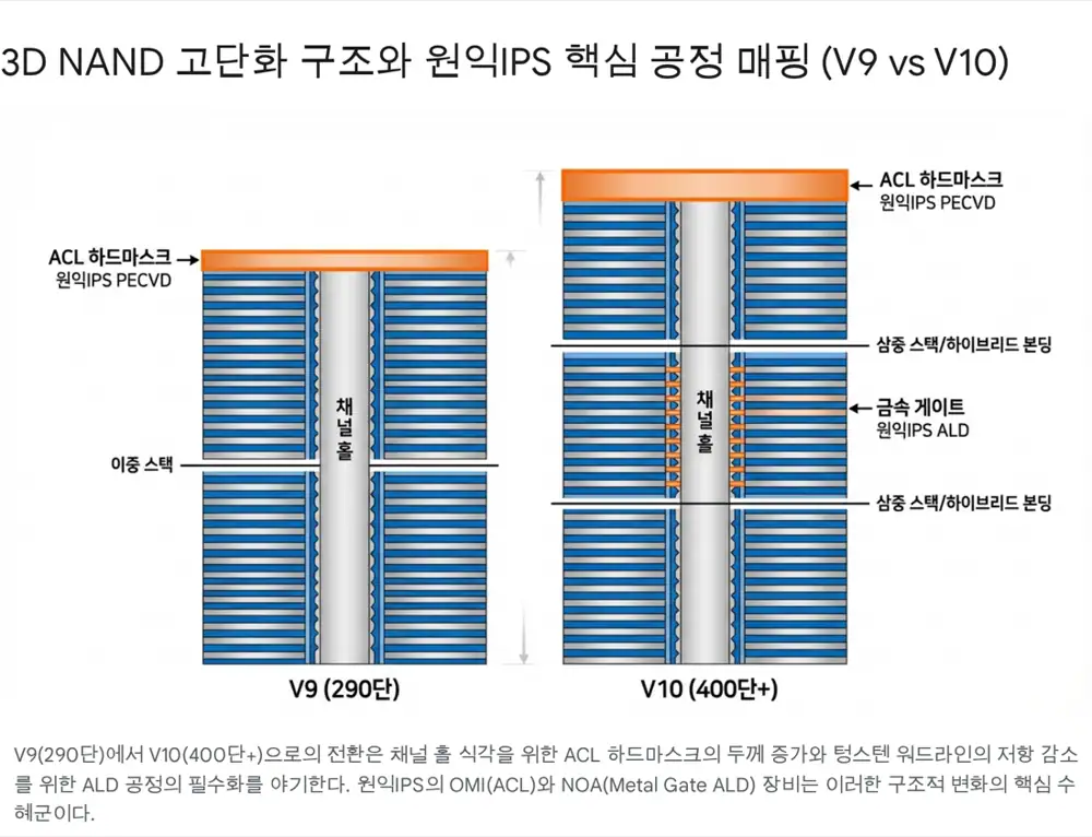
2.1. The HARC etch enabler: ACL hardmask (PECVD)
Above 300 layers, channel-hole etching difficulty rises exponentially. To etch deep, narrow holes vertically through long plasma exposure, a robust protective layer — the hardmask — is essential.
- Bottleneck: Conventional amorphous carbon layer (ACL) hardmasks erode under long etch times, causing bowing and twisting. For V10 (400+ layer) NAND, the hardmask must be thicker or significantly harder.
- Wonik IPS solution: The company's PECVD tools (OMI series, etc.) deposit high-density ACL films with diamond-like properties via high-temperature processes. Above 300 layers, hardmask thickness must increase 30–50% versus legacy, extending tool process time per wafer and structurally raising the required equipment count (Q).
- Quantitative effect: When layer counts rise 1.5x from 200 to 300 layers, hardmask deposition chamber demand grows roughly 1.8–2.0x — non-linear growth. Throughput losses from depositing thicker films uniformly require still more tools.
2.2. Solving wordline resistance: Metal Gate ALD
As 3D NAND stacks taller, wordline electrodes controlling each cell become thinner, raising resistance and slowing NAND operation speed.
- Technical solution: Conventional CVD tungsten (W) deposition struggles to gap-fill thin internal structures and adds resistance from impurities. High-quality ALD-based tungsten and barrier metal deposition becomes essential.
- Wonik IPS edge: The company's NOA (New Orion ALD) and GEMINI systems deliver outstanding step coverage deep inside complex 3D structures. As V9/V10 wordline counts rise, ALD process steps scale linearly with layer count.
- P and Q rise together: ALD tools command 30–50%+ higher ASPs than CVD tools thanks to higher precision. NAND layering accelerates the CVD-to-ALD tech migration, which is the core driver of mix and margin improvement for Wonik IPS.
2.3. New equipment lineup and competitiveness
CUARTO & CLARO
Next-generation deposition tools with high throughput and film uniformity, optimized for V9/V10 processes.
NOA (Metal Gate ALD)
Specialized for tungsten and TiN deposition, solving the 3D NAND wordline resistance problem. Superior gap-fill and low fluorine (F) content improve device reliability versus competitors.
OMI series
Diamond-class high-density ACL deposition that preserves pattern integrity in HARC etch environments.
3. NVIDIA Rubin & ICMS: The start of a hidden AI NAND cycle
The market is fixated on Rubin GPUs and HBM4. But the "second wave" worth watching is the explosion of AI inference demand and the rediscovery of high-performance NAND flash.
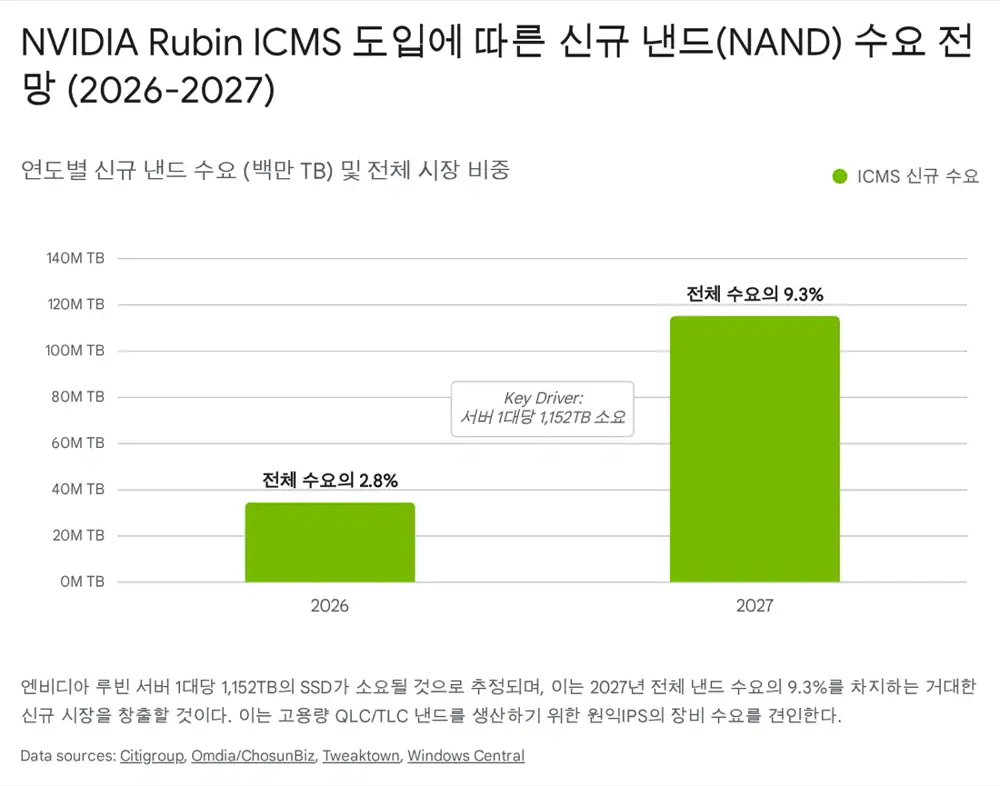
3.1. Agentic AI and ICMS: NAND's return
At his CES 2026 keynote, Nvidia CEO Jensen Huang emphasized Agentic AI and unveiled the ICMS (Inference Context Memory Storage) platform to support it.
- The core problem: When AI models perform multi-step reasoning, the resulting KV cache data exceeds HBM capacity. Scaling expensive HBM or using slow network storage (HDD/SSD) both hit cost and latency limits.
- ICMS: Nvidia's BlueField-4 DPU adds a new high-speed NVMe SSD tier (G3.5) directly connected to the GPU. This requires hundreds of TB to PB-class NAND storage per server and delivers up to 5x higher token throughput and energy efficiency than legacy storage.
- Structural NAND demand: Per Citi Research, Rubin ICMS architecture is estimated to require ~1,152TB of additional SSD per server — about 2.8% of global NAND demand in 2026 and 9.3% in 2027.
3.2. HBF (High Bandwidth Flash) and hybrid bonding
Official fact: Beyond ICMS, a new memory form factor called HBF (High Bandwidth Flash) is emerging. HBF stacks NAND vertically like HBM and applies TSV (Through-Silicon Via) technology to maximize bandwidth, with both Samsung and SK hynix under development.
Interpretation: This is a new catalyst stimulating NAND wafer bonding and stacking equipment demand. Wonik IPS, with its core deposition portfolio across front-end and packaging convergence trends, should benefit over the long term.
4. Key customer value chain and CAPEX trends
Wonik IPS's earnings track Samsung Electronics (SEC) and SK hynix (SKH) investment cycles — especially the tech migration timeline.
4.1. Samsung: P4 phase resumption and V9/V10 transition
From 2024 to early 2025, Samsung's investment was concentrated in HBM-centric DRAM. But signals of change since 2H25 are clear.
- P4 (Pyeongtaek Fab 4) NAND restart: Suspended P4 NAND equipment investment is being resumed from late 2025. It is a necessary response to the explosion in AI server eSSD demand. P4 will be the launching pad for V9 and next-generation V10 NAND, and Wonik IPS plans to supply its core Mold CVD, ACL Hardmask and Metal Gate ALD tools at scale.
- V9 migration: As V7/V8 lines at Xi'an and Pyeongtaek migrate to V9, retrofit and new equipment demand has emerged. Wonik IPS holds the No. 1 share in NAND deposition tools inside Samsung, so it captures the largest share of this transition.
4.2. SK hynix and display/foundry
- SK hynix: M15X fab investment is becoming visible, with tool POs expected from 4Q25. The company's 4D NAND advancement increases the likelihood of Wonik IPS ALD tool adoption, supporting customer diversification.
- Display: Chinese panel makers' Gen 8.6 OLED investment and Samsung Display's IT OLED transition drive display equipment revenue from 2H25, smoothing semiconductor cycle volatility.
CAPEX timeline and order recognition:
- 4Q25: Samsung P4 NAND advance orders and SK hynix M15X initial orders begin.
- 1Q–2Q26: P4 equipment move-in accelerates and tech migration revenue recognition peaks (the earnings quantum-jump period).
5. Financial fundamentals and consensus
After a 2023 trough with operating losses, Wonik IPS returned to profit in 2024 and entered a full earnings-recovery phase in 2025.
5.1. Earnings trajectory and outlook (KRW bn)
| Item | 2023 (A) | 2024 (A) | 2025 (E) | 2026 (E) |
|---|---|---|---|---|
| Revenue | 690 | 748 | 930 | 1,250 |
| Operating profit | -18 | 11 | 98 | 162 |
| OPM (%) | -2.6% | 1.4% | 10.5% | 13.0% |
| Net income | -14 | 21 | 86 | 135 |
(Source: company IR materials and major brokerage consensus, restructured)
5.2. 4Q25 preliminary results review
- Revenue: ~KRW 294.8bn (YoY +30.8%).
- Operating profit: ~KRW 25.9bn (YoY +115.6%).
- Analysis: Slightly below consensus, but driven by typical year-end employee bonuses and one-off costs. What matters is the large YoY volume growth, confirming that NAND and display tool move-ins are normalizing. The NAND revenue mix recovering to DRAM levels thanks to P4 is the key signal for 2026.
5.3. Earnings turning point forecast
The explosive turning point we focus on is 1Q26. P4 and M15X tools ordered in late 2025 begin to be recognized as revenue (delivery basis), while high-capacity eSSD NAND mass production aligned with Nvidia's Rubin launch ramps in parallel.
6. Key risks and bear case
Investors must recognize structural risks behind the rosy outlook.
6.1. Technical risk: the cryogenic etching paradox
Cryogenic etching, under development by Samsung Electronics and Tokyo Electron (TEL), performs etch below -70°C to improve etch speed and form passivation layers — a next-generation technology.
Threat
If cryogenic etch lifts etch selectivity dramatically, the need for thick ACL hardmasks could shrink, slowing the volume (Q) growth of ACL deposition tools.
Mitigation
Above 400 layers, etching deeper and straighter is the primary mandate. Cryogenic etch is more likely an enabler that makes previously impossible depths possible, rather than a tool that reduces hardmask need.
Deposition TAM up
Total deposition equipment TAM still rises with NAND output growth.
6.2. Heightened competition and CAPEX delays
- Competitors: Lam Research (US) and Tokyo Electron (Japan) are formidable competitors. New ALD metal deposition tools from Lam Research in particular could threaten Wonik IPS's share.
- Investment delay: Excessive concentration on HBM means legacy NAND investment could proceed more slowly than expected (bear case). If NAND price increases stall, Samsung may again throttle P4 NAND investment.
7. Valuation and final strategy
7.1. Valuation assessment
Wonik IPS currently trades at ~15x PER and 1.3x PBR on 2026E earnings.
- Historical band: During NAND big-cycle peaks (2017, 2021), the company traded at 15–20x PER and above 2.0x PBR. The current price reflects the early stage of a NAND recovery, but the premium for 2026's structural growth (AI eSSD + V10 layering) is not yet fully priced in.
- Upside: Applying a target PER of 20x (boom-period average) to 2026E EPS implies 30–40%+ upside from the current price.
7.2. Final investment view: BUY (Overweight)
Wonik IPS is more than an equipment supplier — it is a core partner solving the data-storage problem the AI era demands. Nvidia's ICMS strategy points to a long NAND-industry upcycle, and that is a once-in-a-cycle opportunity for the company.
7.3. Key monitoring KPIs
- Samsung P4 NAND tool PO disclosures: Large-scale orders for the P4 line, especially concentrated in 4Q, will be the signal flare for the earnings quantum jump.
- Nvidia Rubin/ICMS-related eSSD demand data: News showing sharp uptake of high-capacity (64TB, 128TB) SSDs in AI servers directly translates to higher utilization of Wonik IPS's 3D NAND tools.
This report is based on public information, and the investment responsibility rests with the investor.
Sources
- Original Naver Blog post: https://m.blog.naver.com/PostView.naver?blogId=star_of_self&logNo=224182187547
- NVIDIA BlueField-4 Powers New Class of AI-Native Storage Infrastructure: https://nvidianews.nvidia.com/news/nvidia-bluefield-4-powers-new-class-of-ai-native-storage-infrastructure-for-the-next-frontier-of-ai
- Introducing NVIDIA BlueField-4-Powered ICMS Platform: https://developer.nvidia.com/blog/introducing-nvidia-bluefield-4-powered-inference-context-memory-storage-platform-for-the-next-frontier-of-ai/
- 3D NAND Hits 400+ Layers with Hybrid Bonding - ALLPCB: https://www.allpcb.com/allelectrohub/3d-nand-hits-400-layers-with-hybrid-bonding
- Flash memory breaks through 400 layers - EEWORLD: https://en.eeworld.com.cn/mp/Icbank/a393685.jspx
- Process Optimization of Amorphous Carbon Hard Mask (ResearchGate): https://www.researchgate.net/publication/352229598_Process_Optimization_of_Amorphous_Carbon_Hard_Mask_in_Advanced_3D-NAND_Flash_Memory_Applications
- Role of Oxygen in ACL Plasma Etching - PMC/NIH: https://pmc.ncbi.nlm.nih.gov/articles/PMC10500572/
- Process Optimization of ACL - MDPI: https://www.mdpi.com/2079-9292/10/12/1374
- Surface Analysis of Amorphous Carbon Thin Film: https://www.researchgate.net/publication/348819201_Surface_Analysis_of_Amorphous_Carbon_Thin_Film_for_Etch_Hard_Mask
- WONIK IPS Product (Semiconductor): https://www.ips.co.kr/cn/business/product.php?board_code=product&product_category=Semiconductor&page_type=view&idx=338
- Process Optimization of ACL - Semantic Scholar: https://pdfs.semanticscholar.org/384d/42b826979950b4f3f027e509154355786ad3.pdf
- Considerations for Improving 3D NAND - Entegris: https://www.entegris.com/content/dam/web/resources/white-papers/whitepaper-improving-3d-nand-performance-8443.pdf
- 3D NAND Channel Hole Deposition Process Control - Chipmetrics: https://chipmetrics.com/applications/3d-nand-channel-hole-deposition-process-control/
- How ALD Impacts Logic & Memory Industries - SEMI.org: https://www.semi.org/sites/semi.org/files/2022-11/06_MichaelGivens_ASMInt.pdf
- NOA ALD - WONIK IPS: https://www.ips.co.kr/en/mo/business/product.php?board_code=product&product_category=Semiconductor&page_type=view&idx=376
- NOA CVD - WONIK IPS: https://www.ips.co.kr/jp/mo/business/product.php?board_code=product&product_category=Semiconductor&page_type=view&idx=337
- Wonik IPS (240810) - KB Securities Research: https://rdata.kbsec.com/pdf_data/20250828194349340E.pdf
- Improving Inference with NVIDIA's ICMS - NAND Research: https://nand-research.com/research-note-improving-inference-nvidias-inference-context-memory-storage-platform/
- ICMSP with Solidigm SSDs and KV cache: https://www.solidigm.com/products/technology/icmsp-ai-inference-is-flash-storage-problem.html
- What NVIDIA's ICMS Means for NAND - Tiger Brokers: https://www.itiger.com/news/1188485227
- Vera Rubin AI systems to eat up MILLIONS of TB of SSDs - TweakTown: https://www.tweaktown.com/news/109677/oh-no-nvidias-next-gen-vera-rubin-ai-systems-to-eat-up-millions-of-terabytes-of-ssds/index.html
- HBF memory stacks - TechRadar: https://www.techradar.com/pro/samsung-and-sandisk-are-set-to-integrate-rival-hbf-technology-into-ai-products-from-nvidia-amd-and-google-within-24-months-and-thats-a-huge-deal
- HBF to Surpass HBM Demand by 2038 - Chosun: https://www.chosun.com/english/industry-en/2026/02/04/EYUINN5VSJC6PGB3RRZ3NTYACQ/
- SK hynix AI Chip with HBF - TrendForce: https://www.trendforce.com/news/2026/02/12/news-sk-hynix-unveils-ai-chip-architecture-with-hbf-reportedly-boosts-performance-per-watt-by-up-to-2-69x/
- Samsung, SK paths diverge on HBF - Korea Herald: https://www.koreaherald.com/article/10669660
- Wonik IPS cash flow improvement - Dealsite: https://dealsite.co.kr/articles/152245?source=nf
- Samsung Accelerates Pyeongtaek Chip Expansion: https://www.korea-certification.com/en/samsung-accelerates-pyeongtaek-chip-expansion-as-ai-driven-memory-demand-rises/
- Wonik IPS - Eugene Investment & Securities: https://www.eugenefn.com/common/files/amail/20250227_240810_sophie.yim_63.pdf
- Wonik IPS NH target price up - TradingView: https://es.tradingview.com/news/hankyung:fa2f419f865a7:0/
- Financial Information - WONIK IPS: https://www.ips.co.kr/en/ir/financial_information01.php
- Cryogenic Etch Re-Emerges: https://www.cryogenicsociety.org/index.php?option=com_dailyplanetblog&view=entry&category=industry-news&id=244:cryogenic-etch-re-emerges
- Cryogenic Etching - TEL Blog: https://www.tel.com/blog/all/20241021_001.html
- Cryogenic Etch: A Key Enabler Of 3D NAND - Semiconductor Engineering: https://semiengineering.com/cryogenic-etch-a-key-enabler-of-3d-nand/
- Samsung, SK hynix cut NAND output to drive profits - ChosunBiz: https://biz.chosun.com/en/en-it/2026/01/20/DV3PLTDTQBBWBKRYAEEJGHFGBY/
- KQ:240810 Financials - Investing.com: https://www.investing.com/equities/wonik-ips-co-ltd-financial-summary
- Wonik IPS Key Metrics - Morningstar: https://www.morningstar.com/stocks/xkrx/240810/key-metrics