DEEP RESEARCH · IMAGE SENSORS / SAMSUNG VS SONY
Samsung Electronics vs Sony Image Sensors: Value Chain Map for the Visual Intelligence Era
From CCD to CMOS, BSI, stacked sensors, 2-Layer Pixel, ISOCELL, ALoP, automotive, and SWIR
0. Bottom line first
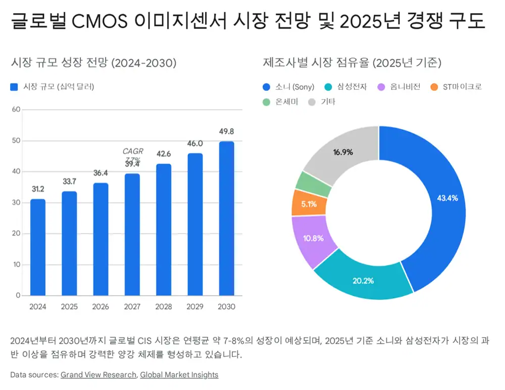
Image-sensor competition is no longer just a smartphone megapixel race. Sony protects the premium market with roughly 45-50% global share, Apple's supply chain, and BSI, stacked, and 2-Layer Pixel technology. Samsung is the No. 2 player at around 20% share, pursuing ISOCELL, 200MP sensors, ALoP, and automotive ISOCELL Auto.
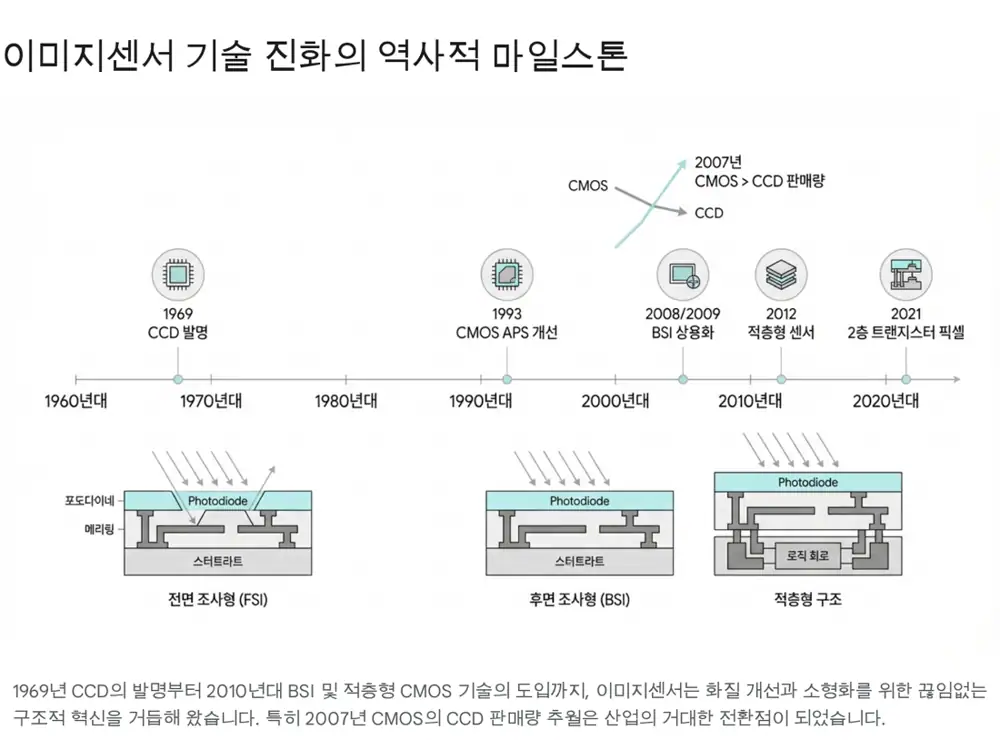
Official fact: The source lists major inflection points: CCD invention at Bell Labs in 1969, Kodak's first digital camera in 1975, CMOS sales overtaking CCD around 2007, Sony's 2012 commercialization of the first stacked CMOS image sensor, and Sony's 2021 announcement of 2-Layer Transistor Pixel.
Interpretation: Sony's edge comes from pixel physics and customer lock-in, while Samsung's counterattack comes from process technology, vertical integration, and module form-factor innovation. From an investment lens, the ecosystem matters: testing, OSAT, and camera modules can benefit alongside sensor designers.
1. Technology history: from CCD to CMOS
The history of image sensors is a push for efficiency and integration. CCD transfers photo-generated charge sequentially through a bucket-brigade structure and converts it to voltage at the output stage. Low noise and high image quality made CCD dominant in broadcast cameras, medical devices, and high-end digital cameras through the 1980s and 1990s.
CMOS reads signals at each pixel by integrating amplifiers and conversion circuitry. It can use standard semiconductor processes, integrate ADCs and ISPs on one chip, and consume less power. NASA JPL's APS work, semiconductor scaling, and noise-reduction technology made CMOS the mobile-era standard.
Starting point of high image quality
Willard Boyle and George Smith at Bell Labs invented CCD in 1969. Kodak's first digital camera used CCD in 1975, and Sony built the Handycam-era peak.
Mobile standard
Low power, miniaturization, peripheral-circuit integration, and mass production are the strengths. CMOS began overtaking CCD sales around 2007 as smartphones spread.
Sony's structural innovation
BSI lets light reach the photodiode without passing through wiring. Sony's 2012 stacked CMOS separated pixel and logic layers to raise performance.
2. Samsung vs Sony: share and customer portfolio
| Item | Sony | Samsung Electronics |
|---|---|---|
| Market position | About 45-50% global image-sensor revenue share in 2024 | About 20% share, No. 2 globally |
| Core customers | Exclusive supplier position for Apple's iPhone series is the stable revenue source | Galaxy is the core captive demand source; Xiaomi, Vivo, Oppo, and other Chinese OEMs diversify the base |
| Brands/products | Exmor, LYTIA, and high-value markets such as mirrorless, broadcast, and security cameras | ISOCELL and commercialization of 100MP and 200MP sensors |
| Supply chain | Strengthens logic production through TSMC and the Kumamoto JASM fab | Vertically integrated System LSI design and Samsung Foundry manufacturing, with some mature nodes outsourced |
3. Pixel-structure war
The two companies are competing to overcome the physical limits of pixels and maximize light capture.
2-Layer Transistor Pixel
Announced in 2021. Sony separates the photodiode layer and transistor layer onto different substrates and stacks them vertically. The source says this expands photodiode capacity, roughly doubles full-well capacity, and reduces noise. It is described as used in iPhone 15/16 series and Xperia 1 V.
ISOCELL and 200MP
Samsung reduces crosstalk by building physical barriers between pixels, then improves light loss through ISOCELL 2.0 and ISOCELL Plus. It has deployed 0.6μm and 0.5μm-class pixels and HP1, HP2, HP3, and HP9 200MP products.
ALoP vs folded zoom
Samsung's ALoP places lenses horizontally above the prism to increase aperture and improve night quality while lowering module height.
Official fact: The source describes Samsung's pixel binning as combining 4 pixels (Tetrapixel), 9 pixels (Nonapixel), or 16 pixels (Tetra2pixel) into one larger pixel. It raises sensitivity in low light while preserving resolution in bright scenes.
4. Beyond mobile: automotive and specialty sensors
As mobile matures, Sony and Samsung are expanding into automotive, industrial sensors, and non-visible-light sensing.
| Market | Sony strategy | Samsung strategy |
|---|---|---|
| Automotive | Creates sensor demand through the Afeela EV project with Honda and works with Mobileye and NVIDIA. It targets Tier 1 suppliers with sensors such as IMX828 and ISX038 and MIPI A-PHY integrated into the sensor. | Uses ISOCELL Auto and CornerPixel to provide over 120dB HDR and LED flicker mitigation. The source mentions references with Tesla HW 4.0/5.0, Hyundai Motor, and Mobileye. |
| SWIR | Launched IMX990/991 high-resolution SWIR sensors using Cu-Cu hybrid bonding to reduce pixel pitch below 5μm, targeting wafer inspection and food contaminant sorting. | The source focuses less on Samsung's own SWIR products and more on challengers such as Aeluma using compound-semiconductor integration on silicon wafers. |
| On-sensor AI | Intelligent Vision Sensor integrates AI processing into the sensor to reduce data transfer, protect privacy, and enable real-time inference. | Samsung expands the sensor and system-semiconductor ecosystem through automotive and mobile platforms. |
5. Value chain: from sensor chip to camera module
The image-sensor industry connects IDMs, fabless companies, foundries, OSAT providers, and camera-module makers. Sony and Samsung both internalize sensor design and front-end manufacturing, but their logic, test, and module ecosystems differ.
| Stage | Companies | Role in the source |
|---|---|---|
| OSAT/test | Doosan Tesna | Top vendor for Samsung CIS wafer testing with high share, investing in equipment amid reports of Samsung expanding Apple CIS supply |
| OSAT/test | LB Semicon | Moved beyond DDI back-end work into Samsung CIS and AP testing as a second vendor, investing in the Anseong plant |
| OSAT/test | Nepes and Nepes Ark | Strong in PMIC packaging and testing, while continuing to explore entry into CIS testing as Samsung's system-semiconductor ecosystem expands |
| Sony back end | KYEC, ASE Technology | Sony is expanding global OSAT cooperation as production volumes rise, despite historically preferring in-house back-end work |
| Camera module | LG Innotek | Strong in iPhone Pro/Max modules, sensor-shift OIS, folded zoom, and iPhone 16 tetraprism modules |
| Camera module | Samsung Electro-Mechanics | Core Galaxy S-series module supplier, expanding automotive camera modules for Tesla and expected to help modularize ALoP |
| Camera module | Sunny Optical | Chinese optical-components player expanding from price-competitive low/mid markets toward premium supply chains |
6. Overall view
Even if smartphone growth slows, image sensors can keep growing because demand to replace the human eye is expanding. In mobile, larger sensors and ALoP-like form-factor innovation matter. In automotive, Level 3+ autonomy raises requirements for HDR, LFM, and sensor counts. At the edge, on-sensor AI becomes central.
My conclusion is that Sony remains the structural leader in premium sensors, while Samsung is attacking through process technology, resolution, module architecture, and automotive references. Investors should not stop at the two sensor makers; they should also track ecosystem bottleneck solvers such as Doosan Tesna, LB Semicon, Nepes, LG Innotek, and Samsung Electro-Mechanics.
Sources
- Original blog: https://m.blog.naver.com/PostView.naver?blogId=star_of_self&logNo=224125356285
- Source 1: https://www.fortunebusinessinsights.com/cmos-image-sensor-market-113742
- Source 2: https://www.grandviewresearch.com/industry-analysis/image-sensors-market
- Source 3: https://ericfossum.com/Articles/Cumulative%20Articles%20about%20EF/Micron%20White%20Paper%20on%20CCDs%20and%20CMOS.pdf
- Source 4: https://petapixel.com/2025/02/03/the-60-year-history-of-digital-image-sensors-as-told-by-those-involved/
- Source 5: https://www.forzasilicon.com/about-us/company-profile/history-of-digital-imaging
- Source 6: https://ptacts.uspto.gov/ptacts/public-informations/petitions/1550798/download-documents?artifactId=yhB3rv3S9ZtjHs_ffgrIRjmozfg1dfa9S1Q2rPWbNqWHXnZ7CaSYOb4
- Source 7: https://en.wikipedia.org/wiki/Image_sensor
- Source 8: https://www.global-imi.com/blog/image-sensors-their-peak
- Source 9: https://www.sony-semicon.com/en/technology/is/back-illuminated.html
- Source 10: https://semiengineering.com/scaling-cmos-image-sensors/
- Source 11: https://en.eeworld.com.cn/news/MEMS/eic703983.html
- Source 12: https://www.gminsights.com/industry-analysis/image-sensor-market
- Source 13: https://library.techinsights.com/search/sectioned-blog-viewer/4835f548-3260-4804-9a68-d727e9a8c205
- Source 14: https://www.sony-semicon.com/en/news/2024/2024020601.html
- Source 15: https://www.kedglobal.com/electronics/newsView/ked202507140001
- Source 16: https://semiconductor.samsung.com/news-events/tech-blog/samsungs-chips-capturing-our-light-filled-world/
- Source 17: https://www.sony-semicon.com/en/technology/mobile/2-layer-pixel.html
- Source 18: https://www.sony-semicon.com/en/news/2021/2021121601.html
- Source 19: https://petapixel.com/2024/08/05/sonys-stacked-sensor-promises-improved-smartphone-image-quality/
- Source 20: https://semiconductor.samsung.com/news-events/tech-blog/taking-unforgettable-photos-with-your-smartphone-all-about-image-sensors-that-determine-the-quality-of-your-photos/
- Source 21: https://images.samsung.com/is/content/samsung/assets/global/ir/docs/2025_1Q_Interim_Report.pdf
- Source 22: https://www.gizmochina.com/2025/11/29/how-does-sonys-200mp-sensor-compare-to-samsungs/
- Source 23: https://isocellsolution.samsung.net/redmine/projects/promo-alop
- Source 24: https://semiconductor.samsung.com/news-events/tech-blog/ces-innovations-awards-2025-honoree-interview-alop/
- Source 25: https://www.sony-semicon.com/en/news/2025/2025102801.html
- Source 26: https://www.sony-semicon.com/en/news/2024/2024100401.html
- Source 27: https://semiconductor.samsung.com/news-events/tech-blog/new-isocell-image-sensor-optimized-for-vehicular-cameras/
- Source 28: https://www.hyundainews.com/releases/4254
- Source 29: https://www.kedglobal.com/korean-chipmakers/newsView/ked202412180013
- Source 30: https://www.sony-semicon.com/en/products/is/industry/swir/imx990-991.html
- Source 31: https://www.sony.com/en/SonyInfo/News/Press/202005/20-036E/
- Source 32: https://www.aeluma.com/investors/news-events/press-releases/detail/64/aeluma-to-showcase-next-generation-sensor-and-silicon
- Source 33: https://www.swirvisionsystems.com/acuros-vs-sony/
- Source 34: https://www.sony-semicon.com/en/news/2021/2021110901.html
- Source 35: https://www.doosan.com/en/media-center/press-release_view?id=20172383
- Source 36: https://www.digitimes.com/news/a20251020PD207/doosan-testing-samsung-apple-cis.html
- Source 37: https://drive.google.com/open?id=1wAOtcEpmKTqUWepVQi9vLi1b6vnpzzi2LuD6ptp8wzI
- Source 38: https://thelec.net/news/articleView.html?idxno=2751
- Source 39: https://www.digitimes.com/news/a20201116PD200.html
- Source 40: https://www.yolegroup.com/press-release/lg-innotek-sony-sunny-optical-samsung-more-and-more-investments-in-continuous-innovation/
- Source 41: https://matrixbcg.com/blogs/competitors/lginnotek
- Source 42: https://www.yolegroup.com/product/report/smartphone-camera-module-comparison-2024---apple-with-iphone-16/
- Source 43: https://appleinsider.com/articles/24/08/26/apple-taps-lg-innotek-for-all-iphone-16-pro-and-iphone-16-pro-max-tetraprism-lenses
- Source 44: https://news.samsung.com/global/samsung-to-showcase-end-to-end-automotive-solutions-at-iaa-mobility-2023
- Source 45: https://www.sony-semicon.com/en/technology/ivs/index.html