DEEP RESEARCH · YC CORP.
YC Corp.: Samsung's Test-Infrastructure Partner in the HBM Catch-up Race
A structured review of memory wafer testers, Samsung's equity stake, MT8311, and the HBM4 opportunity.
0. Bottom line first
My conclusion is that YC is not just another equipment supplier. It is a strategic test-infrastructure partner inside Samsung Electronics' memory ecosystem. Samsung's 11.70% stake, the appointment of president Jang Seong-jin, and the HBM high-speed tester MT8311 all point in the same direction. The key question is whether this strategic position turns into orders and cash flow during the 2025-2026 HBM4 ramp.
1. Roots: Japanese measurement technology plus Korean mass-production capability
Official fact: The source says YC was founded in April 1991 as Koryo Yokogawa Measuring Instruments, the Korean entity of Japan's Yokogawa Electric, and became a technology-owning equipment maker after acquiring Yokogawa's memory tester business in August 2012. It listed on KOSDAQ in 2017 and changed its name from YIK to YC Corp. in March 2024.
Interpretation: That history explains YC's edge. The company internalized Japanese precision-measurement know-how and then adapted it to the mass-production requirements of Korean memory customers.
Memory wafer testers
They electrically test DRAM and NAND Flash wafers and support bad-die sorting and repair processes.
SEMCNS ceramic substrates
Ceramic substrates for probe cards determine the quality of fine-signal transfer between tester and wafer.
Korea-Japan research network
Pangyo, Asan, Tokyo Shinagawa, and Shizuoka Hamamatsu sites cover hardware, ASIC, and software development.
2. Meaning of Samsung's equity investment
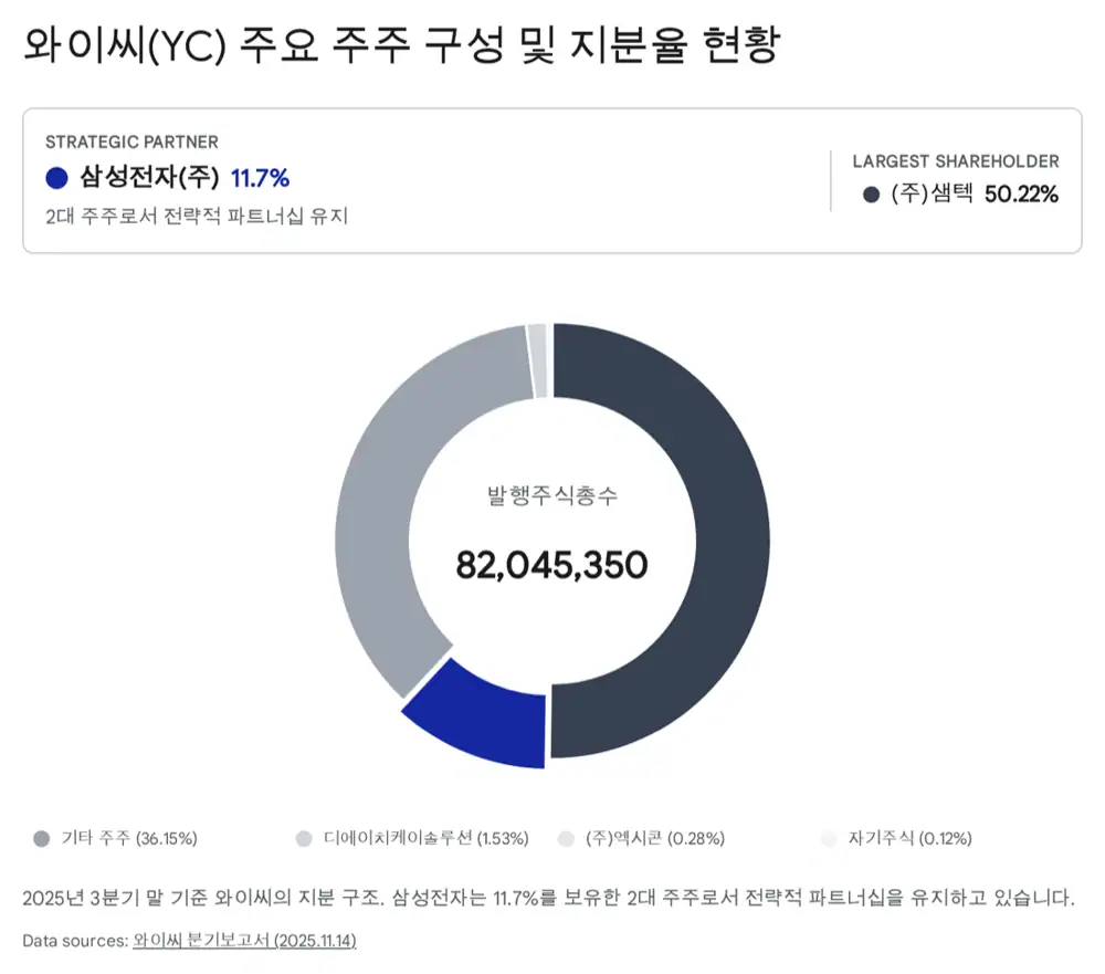
Official fact: Samsung Electronics is presented as YC's second-largest shareholder, holding 11.70% as of the end of Q3 2025.
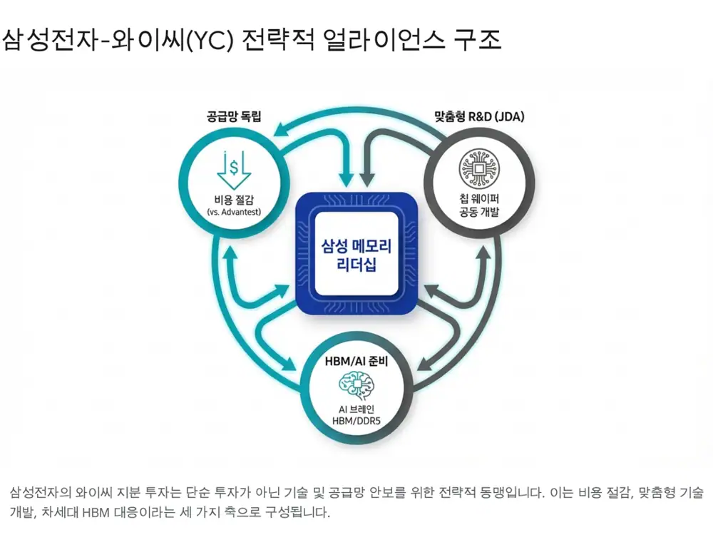
The source's central point is that the stake is not just capital cooperation. It is a strategic device connecting supply-chain security, joint development, and the HBM yield race. After Japan's 2019 export controls on semiconductor materials, Samsung had reason to reduce excessive dependence on foreign test-equipment suppliers such as Japan's Advantest.
The source says YC has long worked with Samsung through JDA, or joint development agreements, from early stages of next-generation memory development. Below-10nm scaling, 300-plus-layer 3D NAND, and HBM-style heterogeneous integration make customer-customized tools more valuable than generic inspection equipment.
3. Product portfolio: MT6122, MT6133, MT8311
| Product/axis | Role in the source | Investment point |
|---|---|---|
| MT6122 | NAND wafer tester. The source says it was jointly developed with Samsung from 2016 and became a standard tool at Samsung's Xi'an and Pyeongtaek NAND lines. | As 3D NAND moves to 200 and 300 layers, detecting cell interference and leakage becomes more important. |
| MT6133 | DRAM wafer tester. Described as used in DDR4 and LPDDR5 mass-production lines. | High-speed clocks and repair accuracy connect directly to DRAM yield improvement. |
| MT8311 | HBM high-speed tester. The source gives maximum 333MHz frequency and 666Mbps data processing speed. | As KGD sorting for HBM core dies grows, its strategic value rises. |
| Advantest T5503HS2 | Global competing tool with 4.5GHz-9Gbps-class performance. | It is strong in final package testing, but YC is framed as a cost, delivery, and service alternative at the wafer stage. |
Interpretation: HBM requires near-perfect sorting of individual core dies before stacking. One bad die can force the disposal of an expensive package, making wafer-stage testing a yield bottleneck in AI memory.
4. Financials: revenue recovery, profit burdened by investment
Official fact: The source reports consolidated Q3 2025 cumulative revenue of KRW 185.9bn, up 26.2% YoY; operating profit of KRW 7.7bn, down 18.4% YoY; and net profit of KRW 8.7bn, down 53.4% YoY. Total assets are described at about KRW 570bn, and the credit rating was downgraded from A- to BBB+ in September 2025.
| Item | Source figure | How I read it |
|---|---|---|
| Q3 2025 cumulative R&D | KRW 20.6bn, 11.1% of revenue | Development burden for next-generation HBM and DDR5 testers |
| 2024 R&D | KRW 23.8bn, 11.3% | R&D ratio moved into the 11% range |
| 2023 R&D | KRW 23.1bn, 9.1% | About 10% of revenue has continued to be reinvested |
| Employees | 130 of 192 employees, about 68%, were research and technical staff at end-2023 | A typical technology-intensive equipment company |
Interpretation: Short-term profit pressure and the credit downgrade are real burdens. The source, however, frames them as growing pains from facilities investment and inventory expansion before HBM revenue scales.
5. 2025-2026 watch points
HBM4 ramp
The source frames late 2025 through 2026 as the start of HBM4 mass production. HBM4 raises testing complexity with 16-plus stacks and foundry logic-die processes.
MT8311 adoption
As stack count rises, full inspection of core dies becomes more important, supporting demand for YC's high-speed tester.
Advantest lead times
The longer global tool lead times and higher prices become, the more incentive Samsung has to raise YC's share.
6. Risks and my conclusion
- Single-customer risk: YC is heavily dependent on Samsung, so Samsung's HBM competitiveness and CAPEX decisions can move YC's earnings sharply.
- Customer diversification: SK hynix already has a firm Advantest-centered ecosystem, making entry difficult.
- Technology gap: Advantest is a strong competitor with 9Gbps-class testers. YC must narrow or hold the gap through HBM4E and HBM5.
My view is straightforward. YC is a test logistics base in Samsung's effort to regain HBM leadership. The more important signal is not the Q3 2025 profit slowdown, but whether Samsung succeeds with HBM4 supply to Nvidia and whether YC's equipment purchase orders follow.
Sources
- Source 1: Original Naver Blog post · https://m.blog.naver.com/PostView.naver?blogId=star_of_self&logNo=224125331515
- Source 2: Memory Wafer Tester 2025-2033 Market Analysis · https://www.marketreportanalytics.com/reports/memory-wafer-tester-374025
- Source 3: Advantest Competitive Landscape - PESTEL Analysis · https://pestel-analysis.com/blogs/competitors/advantest
- Source 4: ADVANTEST Risk Factors · https://www.advantest.com/en/investors/management-policy/risk/
- Source 5: Samsung Electronics history - EVOLOG · https://www.evolog.in/samsung-electronics-history
- Source 6: Edaily: YC president Jang Seong-jin and Haedong Technology Award · https://www.edaily.co.kr/News/Read?newsId=04096726642397208&mediaCodeNo=257
- Source 7: IB Tomato: Samsung semiconductor investment losses · https://www.ibtomato.com/mobile/mView.aspx?no=14712
- Source 8: Goover: YC company report · https://seo.goover.ai/report/202512/go-public-report-ko-f7b684da-c55b-45e3-9414-47805321185e-0-0.html
- Source 9: YC news: MT6122 100th shipment · https://yccorp.com/kr/pr/news.php?bgu=view&idx=187
- Source 10: ADVANTEST T5503HS2 product specifications · https://www.advantest.com/en/products/semiconductor-test-system/memory/t5503hs2/
- Source 11: FnGuide YC snapshot · https://comp.fnguide.com/SVO2/ASP/SVD_Main.asp?gicode=A232140
- Source 12: Investing.com: Samsung HBM4 Nvidia test · https://kr.investing.com/news/stock-market-news/article-1763994
- Source 13: NewsQuest: Samsung HBM4 Nvidia test · https://www.newsquest.co.kr/news/articleView.html?idxno=259021
- Source 14: Naver Premium Content: YC company visit · https://contents.premium.naver.com/rvs/tbw/contents/250628133654358vk