DEEP RESEARCH · LB Semicon
LB Semicon: from a DDI house to a SoC test hub
What Exynos 2600, HPB, and the LB Lusem merger imply for the Korean OSAT supply chain
0. Bottom line first
The core view in the source is that the Exynos 2600 wafer-test win can re-rate LB Semicon from a DDI-heavy OSAT into a higher-value SoC test company.
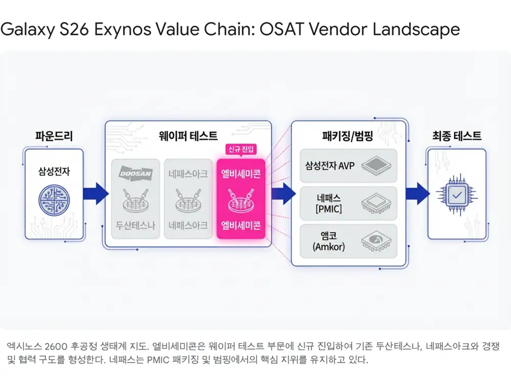
Official fact: The source says LB Semicon was selected in November 2025 as a Samsung Exynos 2600 wafer-test partner. It also treats the February 1, 2025 absorption merger with LB Lusem as a key financial and process event.
Interpretation: Moving beyond a business where DDI represented 70-80% of revenue can change customer mix, technical difficulty, and valuation multiples at the same time.
DDI 70-80%
The traditional revenue base was tied to the display cycle.
Exynos 2600
A symbol of entry into high-reliability AP wafer testing.
2025.02.01
The LB Lusem merger strengthens turnkey bumping, test, and packaging capability.
1. Front-end change, back-end opportunity
The report frames Samsung Foundry's 2nm SF2 process and HPB as comeback cards after 3nm yield issues and the Exynos 2500 mass-production failure. Exynos 2600 production and the 2026 Galaxy S26 scenario are the starting point for a shift in Korean system-semiconductor back-end work.
Official fact: The source says Samsung Foundry began stabilizing 2nm SF2 yields at the 50-60% level from the second half of 2025 and entered Exynos 2600 production.
Interpretation: 2nm and HPB are not only front-end stories. More test items and longer test time can improve OSAT unit pricing and utilization.
2. Business model and merger synergy
LB Semicon receives finished wafers, forms bumps that connect chips to substrates, tests electrical performance, and sorts known-good die. Gold bumping is the traditional cash cow for LCD/OLED DDI, while solder and Cu pillar bumps are used for AP, PMIC, CIS, and other high-performance non-memory chips.
| Process | Role | Meaning in the source |
|---|---|---|
| Bumping | Forms Au, solder, or Cu protrusions on the die | Electrical connection to substrate or leadframe |
| Wafer test | Uses probe cards to test electrical characteristics | The Exynos 2600 CP test win falls here |
| Back-end assy | Sawing, grinding, WLCSP and related work | Combined with LB Lusem's packaging capability |
Official fact: The merged company is described as a KRW 769.1bn-asset OSAT as of Q3 2025. LB Lusem had strengths in display COF packaging and power-semiconductor back-end processing.
Interpretation: Combining LB Semicon's bumping/test with LB Lusem's packaging/assembly enables turnkey offerings. The merged company's liquidity also supports Exynos test equipment and Anseong expansion CAPEX.
3. Customers and 2023-2025 investment flow
Key customers include LX Semicon, Samsung Electronics, MagnaChip, and Himax. LX Semicon is the major fabless company in the LG Display ecosystem and a large DDI bumping/test source, while Samsung System LSI is the growth axis for Exynos and ISOCELL.
CIS line
Anseong added a CIS test line and cleanroom expansion.
AP testers
Even during the DDI downturn, the company began ordering high-end AP test equipment.
Dedicated setup
After the Exynos 2600 win, Exynos test equipment setup and readiness followed at Anseong.
4. Galaxy S26 scenarios and utilization
The source assumes annual Galaxy S26 series shipments of about 35 million units and about 15-20% Exynos wafer-test share for LB Semicon as a new vendor.
| Scenario | Exynos adoption | Units | LB Semicon utilization read |
|---|---|---|---|
| Bear | 20% | About 7 million | Limited effect if yield remains unstable |
| Base | 30-40% | About 10-14 million | SoC test line could recover to about 75% in H1 2026 |
| Bull | 50%+ | About 17.5 million | 85%+ utilization and possible expansion pressure |
Official fact: Current Q3 2025 non-memory line utilization is described as the mid-60% range because of weak DDI demand.
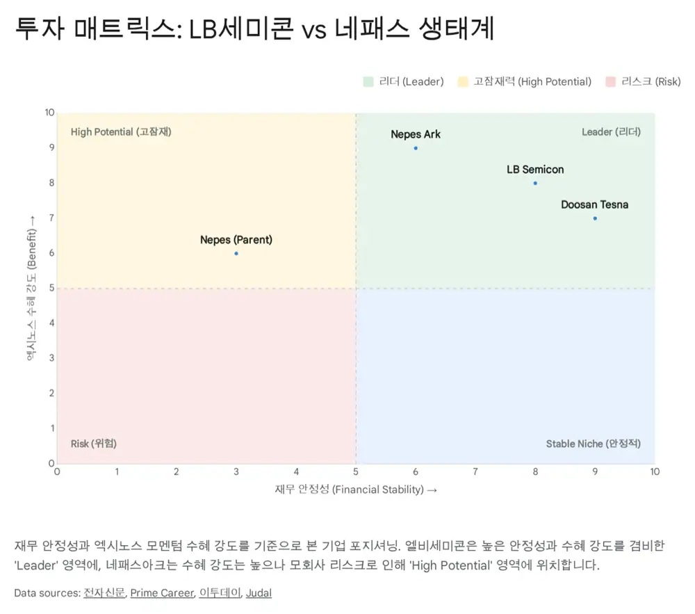
5. Nepes comparison, HPB, and risks
Nepes began in 1990 as a semiconductor materials company and became a first-generation OSAT. In the Exynos ecosystem it has been tied to PMIC, WLP, and FO-PLP. Nepes Lawe, spun off in 2020, invested more than KRW 600bn in a 600mm panel-based FO-PLP facility but fell into capital impairment at end-2023 after yield and customer delays, according to the source.
HPB reduces the heat trap from DRAM stacked above the AP by using a copper heat block or placing AP and DRAM side by side through FOWLP. The source says thermal resistance can fall by more than 30%, while early main AP packaging is likely to be led by Samsung AVP, leaving OSAT opportunities in related components, sub-packaging, and PMIC.
| Valuation or risk | Source number | Checkpoint |
|---|---|---|
| LB Semicon PBR | 0.7-0.8x on 2025 expected earnings | Whether weak DDI is already priced in |
| EV/EBITDA | About 7.7x versus global OSAT average of about 8-10x | Multiple expansion from SoC test entry |
| Re-rating range | 2026 PER below 10x, possible PBR 1.2-1.5x | Exynos volume and merger-effect visibility |
| Risks | 2nm yield, heat/performance issues, delayed IT set recovery | Galaxy S26 Exynos share and DDI utilization |
Interpretation: The source classifies LB Semicon as Top Pick, Nepes Ark as Interest, and Nepes as Watch. I read that as a distinction in risk-adjusted exposure, not as a standalone investment instruction.
Sources
- Original: https://m.blog.naver.com/PostView.naver?blogId=star_of_self&logNo=224123603600
- LB세미콘, 삼성전자 '엑시노스 2600' 테스트 맡는다: https://www.etnews.com/20251121000092
- This Exynos 2600 feature might keep future Snapdragon chips from running hot: https://www.androidauthority.com/samsung-exynos-2600-heat-technology-snapdragon-3624279/
- Samsung's Heat Path Block Technology May Power Cooler Qualcomm and Apple Chips: https://www.towardspackaging.com/news/samsung-heat-path-block-technology-qualcomm-apple
- The Exynos 2600 AP is not hot and that is cool - PhoneArena: https://www.phonearena.com/news/the-exynos-2600-ap-stays-cool-thanks-to-heat-sink_id176551
- [News] Samsung Exynos 2600 May Cover Just 30% of Galaxy S26 Production Amid Reported Yield Issues - TrendForce: https://www.trendforce.com/news/2025/10/24/news-samsungs-exynos-2600-may-cover-just-30-of-galaxy-s26-production-as-2nm-yield-issues-persist/
- Samsung taps LG affiliate LB Semicon for testing Exynos 2600 - RCR Tech: https://rcrtech.com/test-and-measurement-news/samsung-taps-lg-affiliate-lb-semicon-for-testing-exynos-2600/
- 엘비세미콘 (061970KQ | NR): https://ssl.pstatic.net/imgstock/upload/research/company/1593044394456.pdf
- Samsung sets Galaxy S26, Z Fold 8 and Z Flip 8 sales targets for 2026 - Sammy Fans: https://www.sammyfans.com/2025/11/04/samsung-galaxy-s26-z8-foldables-2026-targets/
- Samsung's big 2026 plan shows what it really expects from the Galaxy S26 - PhoneArena: https://www.phonearena.com/news/samsung-big-2026-plan-shows-what-it-really-expects-from-the-galaxy-s26_id175524
- 갤럭시S26 가격 방어 핵심 '엑시노스 2600'…스냅드래곤보다 최대 30달러 저렴 - 케이벤치: https://kbench.com/?q=node/273412
- 네패스, PMIC 패키징 'FO-PLP' 세계 최초 적용 '눈앞' - 디지털데일리: https://m.ddaily.co.kr/page/view/2020110517583436313
- 네패스아크 (KQ.330860) - 성균관대학교 금융투자학회 S.T.A.R: https://www.starskku.com/fileRequest/download?file=%2Fboard%2Fresearch%2F20240311172036_7317.pdf&save=STAR_%E1%84%82%E1%85%A6%E1%84%91%E1%85%A2%E1%84%89%E1%85%B3%E1%84%8B%E1%85%A1%E1%84%8F%E1%85%B3.pdf
- 네패스라웨 분석 | 한국투자PE 포트폴리오 - 프라임 커리어: https://prime-career.com/series_article/298
- '궁지에 몰린' 네패스라웨, 청산 or 매각 - 딜사이트: https://dealsite.co.kr/articles/127285/075033
- 흔들리는 네패스그룹, 네패스야하드 매각도 '험로' - 네이버 프리미엄콘텐츠: https://contents.premium.naver.com/thebell/stock/contents/241230171140971uf
- [특징주] 네패스아크, 16조 규모 AI 정책 기대감⋯엑시노스 파트너 이력 부각에 21% - 이투데이: https://www.etoday.co.kr/news/view/2479907
- [News] Samsung Reportedly Starts Exynos 2600 Mass Production, Yield Estimated to Reach 50% - TrendForce: https://www.trendforce.com/news/2025/09/30/news-samsung-reportedly-starts-exynos-2600-mass-production-yield-estimated-to-reach-50/
- 엑시노스 갤럭시 S26 수혜주 및 ETF 분석: https://drive.google.com/open?id=1WdFQ-9iPbkeQ7RL-pNFdXitFhev6DHdJ6Q7HMR0iLhI
- Samsung's Heat Dissipation Tech For Exynos 2600 Might Soon Feature Within Apple Silicon And Qualcomm's Snapdragon Chips - Wccftech: https://wccftech.com/samsungs-heat-dissipation-tech-for-exynos-2600-might-soon-feature-within-apple-silicon-and-qualcomms-snapdragon-chips/
- 삼성 파운드리 냉각 기술 분석: https://drive.google.com/open?id=1Zb2IhXiHV5Q1WqOS_cvutg5PT45dW0TorCsOS0Pb-EU
- 21 - 주달: https://www.judal.co.kr/?view=stockAI&shareToken=2otLnqzQilJPIKe4
- 엘비세미콘 (A061970) EV/EBITDA - Investing.com: https://kr.investing.com/pro/KOSDAQ:A061970/explorer/ev_to_ebitda_ltm