DEEP RESEARCH · CUSTOM HBM
Custom HBM and Packaging Internalization — SK hynix’s Lead and the Next Competitive Axis
A semiconductor memory memo on custom HBM after HBM4, foundry capability, and FOWLP-based on-device AI memory strategy
0. Bottom line first
In the ASIC market, SK hynix is currently described as the most advanced memory semiconductor company. But if custom HBM becomes serious from HBM4E and HBM5 onward, Samsung Electronics may gain an advantage because it has internalized foundry and advanced packaging capabilities. SK hynix’s response is to internalize packaging technologies such as FOWLP.
Official fact: The source says it was reposted for memory, cites IT God Telegram, and includes The Bell article titled “[Opening of the ASIC era] SK hynix, AI memory strategy: internalizing packaging technology.”
Interpretation: The key issue is not only HBM share today. It is which company benefits when customer-specific requirements, packaging, and foundry capability converge in the next generation.
1. Current advantage: SK hynix HBM reliability
The source describes SK hynix as the memory semiconductor company furthest ahead in the ASIC market because of the high reliability of its HBM products.
- SK hynix is developing and producing products based on HBM element technologies verified through years of mass production.
- Samsung Electronics is described as struggling at the HBM4 development stage.
- SK hynix provided HBM4 12-layer samples to major customers in March this year.
- The source says this was faster than Samsung Electronics and Micron.
2. Custom HBM arrival and share risk
SK hynix has secured time to stabilize HBM4 products and reflect customer requirements. At the time, SK hynix said it had shipped HBM4 12-layer samples earlier than planned based on its technology and production experience in HBM, started customer qualification, and would finish mass-production preparation within the second half.
Competitors, by contrast, are described as not yet supplying HBM4 samples at this point. Samsung Electronics is reportedly targeting HBM4 sample supply within the third quarter according to its internal roadmap.
Official fact: The memory industry expects the custom HBM market to become serious from HBM4E and HBM5, and the source says a senior industry official stated that custom HBM outside JEDEC standards would appear from HBM4E.
Interpretation: Because HBM already has custom-product characteristics, major AI semiconductor companies may prefer using one company’s HBM rather than splitting across multiple memory vendors. This is why winner-take-most dynamics are said to be intensifying.
SK hynix lead
It provided HBM4 12-layer samples to major customers in March and gained time for qualification and stabilization.
HBM4E and HBM5
The industry expects custom HBM to become serious from HBM4E and HBM5.
Foundry capability
Because custom HBM requires foundry capability, Samsung could stand out.
3. Samsung internalization and SK hynix-TSMC cooperation
If custom HBM becomes serious, Samsung Electronics could gain the upper hand because it has internalized foundry and advanced packaging technologies. The reason is that internalized foundry process capability can help Samsung in custom HBM development and commercialization.
SK hynix chose cooperation with an external foundry. From HBM4 onward, it is entrusting base die production to Taiwan foundry TSMC, and this cooperation is expected to expand further in custom HBM.
| Company | Strategy | Meaning in the source |
|---|---|---|
| Samsung Electronics | Internalized foundry and advanced packaging technology | May be advantaged in custom HBM development and commercialization |
| SK hynix | External foundry cooperation with TSMC | TSMC handles HBM4 base die production, with cooperation expected to expand in custom HBM |
4. SK hynix response: FOWLP and on-device AI memory
SK hynix is also internalizing packaging technologies such as FOWLP to maintain leadership in next-generation memory. The source notes that this packaging technology was not used in traditional memory semiconductors.
SK hynix plans to respond to the on-device AI market through FOWLP. It is preparing two types of AI-specialized memory for on-device use.
- Vertical fan-out (VFO) DRAM: characterized by stacking multiple LPDDR55 DRAMs, and sometimes called mobile HBM in the industry. Unlike HBM, however, it does not use a base die that performs logic functions.
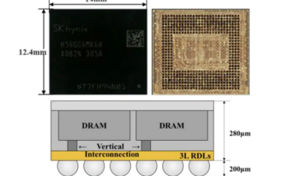
- Dual-die DRAM: a concept that mounts two DRAM dies on a redistribution layer (RDL). With package size around 12.4 x 14mm2 and thickness around 0.48mm, it is expected to be used in applications requiring a thin form factor.
- Both products use FOWLP technology for mass production.
Sources
- The Bell article: https://m.thebell.co.kr/m/newsview.asp?svccode=00&newskey=202506101032418640109556
- IT God Telegram: cited in the source text
- Original Naver blog post: https://m.blog.naver.com/PostView.naver?blogId=star_of_self&logNo=223898466666