DEEP RESEARCH · Silicon photonics
Optical Semiconductors and Silicon Photonics: Reading the Bottleneck Through CPO, COUPE, and SoIC
A study note on optical conversion, advanced packaging, and hybrid-bonding ecosystems for reducing chip-to-chip bottlenecks
0. Bottom line first
Chip-to-chip connection is always a bottleneck. Silicon photonics, which converts electrical signals into light, and CPO, which brings that optical engine into the processor package, are technologies I need to keep watching in AI data centers and high-performance computing.
Official fact: The linked article title says TSMC has opened the competition in optical semiconductors and is building a broad cooperation system. The article summary says TSMC is building a supply chain ahead of next year’s mass production, while Samsung Electronics and Intel are also expected to enter the market.
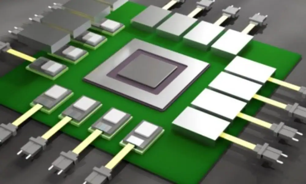
1. Relationship between silicon photonics and CPO
- Silicon photonics is a technology that transmits data by converting electrical signals into light.
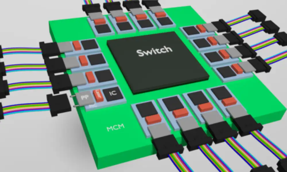
- CPO, or Co-Packaged Optics, integrates a processor or XPU and an optical engine in one package to improve data-transfer efficiency.
- Silicon photonics is a core technology for implementing CPO, while CPO minimizes the physical distance between the processor and optical engine to maximize data-transfer efficiency.
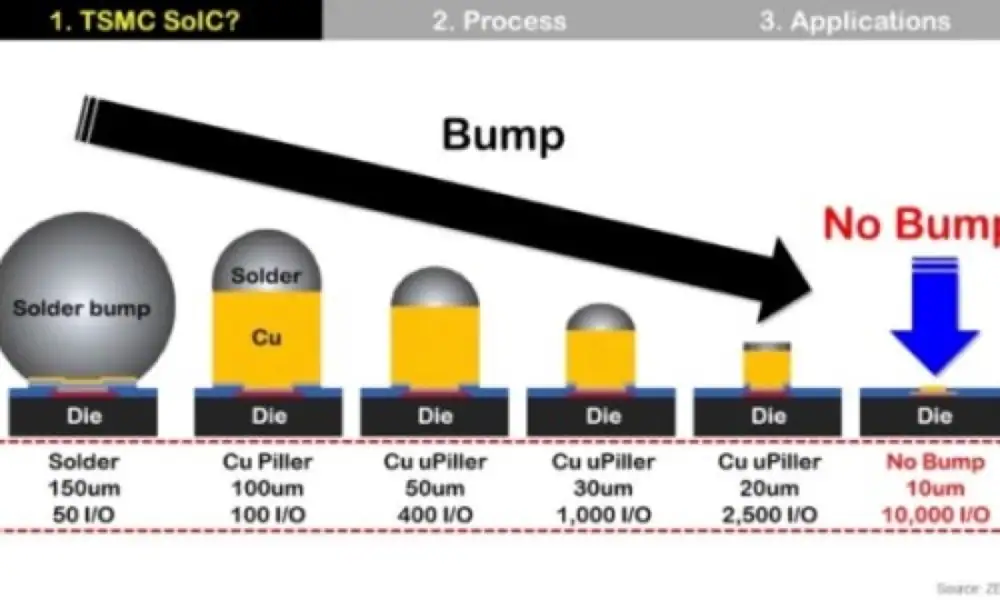
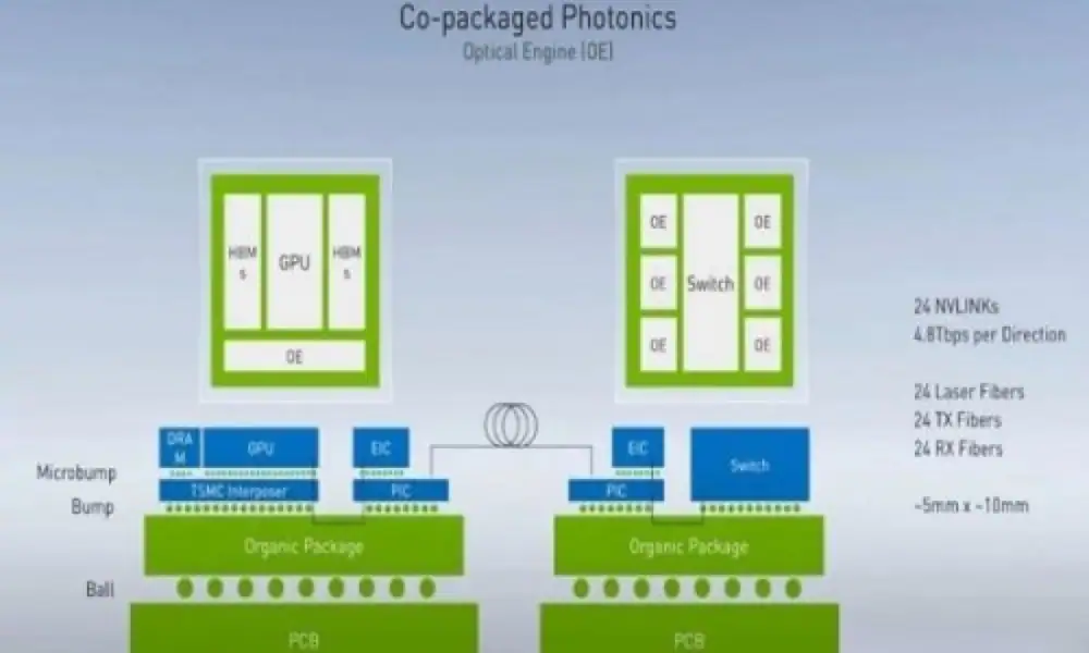
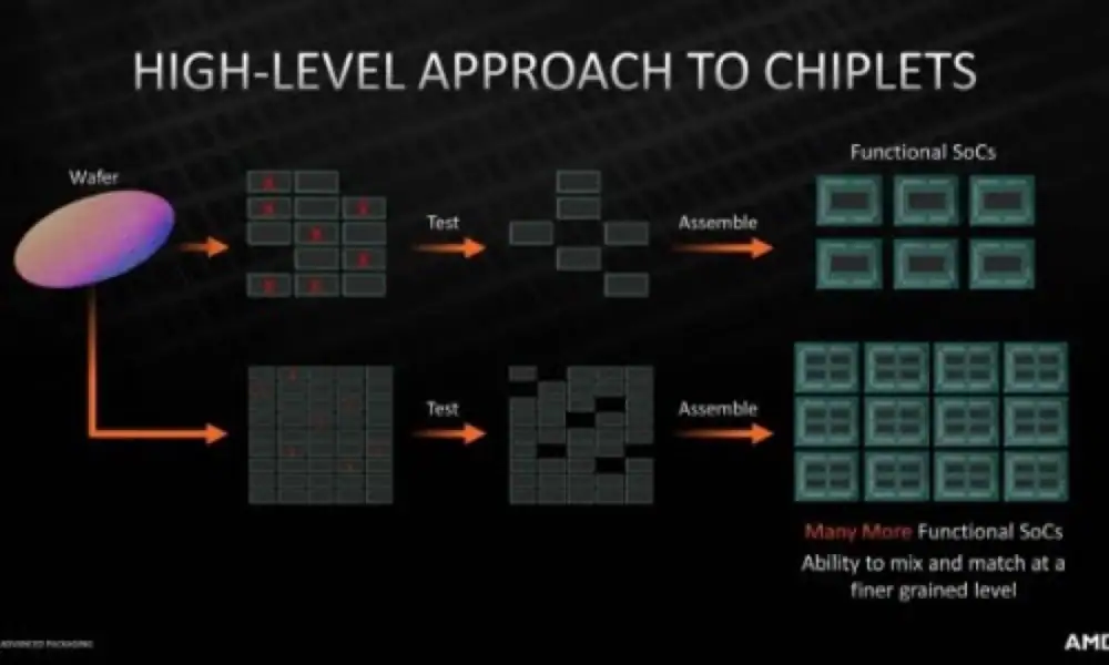
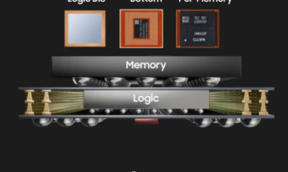
2. How TSMC COUPE connects with SoIC
Compact Universal Photonic Engine
TSMC’s CPO platform integrates electronic integrated circuits, or EICs, and photonic integrated circuits, or PICs, through SoIC-X chip packaging.
System on Integrated Chips
TSMC’s 3D stacking technology uses TSVs without micro-bumps to stack chips vertically and implement high-speed connections.
Dense integration of optics and electronics
COUPE uses SoIC hybrid bonding to integrate electronic and photonic ICs, improving data-transfer efficiency and reducing power consumption.
3. Hybrid bonding process and equipment
| Step | Core content | Related equipment |
|---|---|---|
| Preparation | Deposit insulators and copper wiring on wafers and dies, planarize the surface with CMP, then treat the surface through plasma activation | CMP and cleaning equipment, metrology equipment |
| Bonding | Bond aligned wafers and dies at a set temperature to form bonding between insulating layers | Hybrid bonders and nanometer-level precision metrology tools |
| Annealing | After bonding, use hydrogen annealing to increase bonding strength and remove gaps | Annealing equipment |
| Dicing | Separate the wafer into individual dies | Laser dicing equipment |
4. Major company trends
- NVIDIA entered silicon photonics through its 2020 acquisition of Mellanox and is developing silicon photonics technology for AI data centers in cooperation with TSMC and Broadcom.
- TSMC provides silicon-photonics-based packaging solutions through COUPE and SoIC and is expanding applications in AI and high-performance computing, or HPC.
- Corning supplies silicon-photonics-related components based on optical glass and fiber technology, and the note summarizes a view that Optical revenue will begin in earnest from 2025.
Interpretation: As efficiency improvement becomes more important in data centers and AI computing environments, silicon photonics and related equipment are likely to become more important.
5. Additional references
I am keeping these references on silicon photonics, CPO, SoIC, glass substrates, and FO-PLP together. This topic should be read as a shift toward solving data-movement bottlenecks with packaging and optical conversion, not only with front-end process scaling.


Sources
- Daum News: https://v.daum.net/v/20241229140115615
- TSMC packaging roadmap reference: https://m.blog.naver.com/invesqueeze/223609713634?utm_source=chatgpt.com
- TSMC 3D-SoIC reference: https://m.blog.naver.com/acorn_yun/222606281176?utm_source=chatgpt.com
- OFC 2024 CPO reference: https://www.fibermall.com/ko/news/ofc-2024-cpo-era.htm
- CPO practicality reference: https://www.fibermall.com/ko/blog/practical-co-packaged-optics.htm
- TSMC advanced packaging reference: https://m.blog.naver.com/limnico/222660151981
- Silicon photonics reference: https://m.blog.naver.com/peterlynch7/223210035278
- Glass substrate report reference: https://m.blog.naver.com/keepvividdream/223614135783
- Silicon photonics explainer reference: https://m.blog.naver.com/semi_blog/223269784657
- TSMC 3D stacking reference: https://sciencetech.tistory.com/entry/TSMC%EC%9D%98-3D-%EC%A0%81%EC%B8%B5-%EB%B0%98%EB%8F%84%EC%B2%B4-%EA%B8%B0%EC%88%A0%EC%9D%98-%EC%83%88%EB%A1%9C%EC%9A%B4-%ED%91%9C%EC%A4%80-%EC%A0%9C%EC%8B%9C
- FO-PLP strategy reference: https://sciencetech.tistory.com/entry/%EC%82%BC%EC%84%B1%EC%A0%84%EC%9E%90%EC%99%80-TSMC%EC%9D%98-FO-PLP-%EA%B8%B0%EC%88%A0-%EB%B0%8F-%EC%A0%84%EB%9E%B5%EC%9D%98-%EC%B0%A8%EC%9D%B4
- ETRI material: https://ettrends.etri.re.kr/ettrends/196/0905196002/
- Meeco material: https://meeco.kr/mini/38807299
- Original blog: https://m.blog.naver.com/PostView.naver?blogId=star_of_self&logNo=223708896220